For standard IC testing, we typically need only electrical input and output. Optionally, the measurements are done at different temperatures as well. When it comes to testing MEMS, additional inputs need to be applied or outputs detected (detecting of movements by vision, application of force, light or pressure as example). Depending on the test requirements, the test platform is either in an open or closed environment. Whereas electrical test, electrostatic or over-pressure stimulation can be done on an open platform, other conditions require an enclosed system. This can be a test under vacuum, with different gas concentrations or humidity.
In this post, we’ll cover pressure sensors. There are three possibilities to testing a pressure sensor:
- A static test by applying real pressure with a pressure probe module, or inside a pressure chamber to the entire wafer
- A dynamic test via stimulation with an electrostatic field to extract the mechanical parameters
The pressure probe module applies a static pressure to a single membrane from the top side. The possible test pressure ranges from 100 mbar over pressure to 7 bar relative to atmosphere. The nozzle does not touch the membrane and there will be a gap to the wafer surface of about 40 µm. The alignment of the nozzle to the membrane is done through an optical window integrated into the top side of the nozzle.
The nozzle size is specifically designed to the size of the membrane. To move the nozzle in and out of the microscope view, no pads are required on at least one side of the membrane. In order to not touch the probe needles with the nozzle, a minimum distance of 150 µm is needed between the edge of the membrane and the probe pad. The current minimum nozzle size is 450 µm square. Before testing can be started, different calibration routines are performed. To keep the distance between the pad and nozzle stable, the velocity pressure inside the nozzle is measured while applying pressure. During calibration, pressure to distance curve is measured between touchdown and about 300 µm distance to the wafer. During testing, the velocity pressure can be measured and converted into a distance, and if necessary, the height of the nozzle is corrected. Once this distance is calibrated, the impact pressure will be determined. This is the pressure that effectively bends the membrane. The calibration is done on a calibration area, which is attached to the main chuck of the probe system.
It’s important for wafer-level test that the results are comparable to the final test of the packaged device. The company we are collaborating with compared both results and found that at room temperatures, the results of the on-wafer test and package test are within the specified accuracy of 1 percent. The conclusion here is that testing at wafer level is an advantage in saving the cost of packaging bad dies.
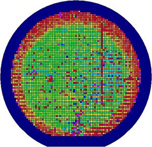
 The image to the right shows the result of an electrical only pressure sensor test, where green is DUT within spec and red is DUT out of spec. The majority of the dies past the test successfully. When a pressure is applied, the results look completely different. In the edge area, the measured sensitivity of the sensor is not within specification. This is due to different membrane thicknesses after the etching process. Therefore, testing with pressure excitation is helpful to detect these differences.
When we think of pressure chambers, we can refer to the PAP200, which is a semiautomatic pressure probe system. It’s based on our vacuum probe system with an extended overpressure capability. The maximum possible pressure is 4 bar absolute. Different chuck temperature options range from -60 °C to 200 °C. Some devices are characterized by using different gas concentrations. Non-aggressive and non-toxic gases can be used with the system.
For a dynamic MEMS test, the movable MEMS part is stimulated by an electrostatic probe card. The resulting movement is detected by optical measurement equipment. To automatically step through the wafer, a semiautomatic probe system is used. The stimulation is done by an electrostatic field. To apply this, a transparent ITO electrode is implemented into a standard size probe card style board. This enables an easy adaptation into standard probe card adapters. The transparent electrode provides a free field of view to the device to align the electrode over the MEMS. The device is brought into close proximity to the electrode but no direct contact is made. A frequency of up to 300 kHz can be applied.
The optical measurement system will detect the resulting frequency response. This response will be compared to the previously done simulation. If the modal frequencies don’t match, the measured (membrane) is not within specification. It can be different in thickness or broken. The real membrane thickness can also be calculated.
The static measurement by applying a pressure and this dynamic approach have been compared. Both results have shown a maximum difference of 5 percent. Therefore, this test can be used as an alternative for static testing. It is also faster because settling time after applying the pressure is not relevant for this test.
Subsequent blog posts will cover microphones, resonators, oscillators and RF switches, and microbolometers. Come back soon!