November 26, 2019
Validated by key automotive manufacturers and deployed to various tester platforms (T2000, V93K DD, J750), the TrueScale Matrix 300mm wafer probe card is meeting the zero-defect challenge.
November 26, 2019
Validated by key automotive manufacturers and deployed to various tester platforms (T2000, V93K DD, J750), the TrueScale Matrix 300mm wafer probe card is meeting the zero-defect challenge.
The automotive semiconductor market is growing quickly, with predictions between 3 and 14% CAGR between 2016 and 2021, reaching $43 billion by 2021. The number of semiconductors in automobiles increases in today’s more modern vehicles thanks in part to critical safety systems, greater fuel efficiency technologies, navigation and communications enhancements, comfort and entertainment features, and autonomous and assisted driving advancements. As a result, we’re seeing the soaring proliferation of radar, LiDAR, and image sensors, RF/mmWave chips, and microcontrollers to help support these new vehicle developments.
The challenge is that IC manufacturers need to adopt a zero-defect requirement protocol in an environment that is naturally challenging. Afterall, vehicles are designed to last 10 years or more (compared to your cell phone as example) and face harsh environmental requirements that an automobile introduces. In addition, wafer test suppliers need to ramp up test coverage without driving up the cost of test.
In a Chip Scale Review article from earlier this year – Automotive IC Production Wafer Test in a Zero-Defect World – our own Amy Leong reflected on this challenge:
Wafer probing is a “contact sport.” The more force the probe puts on the wafer test pad, the greater the chance to create defects to the circuitries underneath the pad. To support a zero-defect manufacturing process, probe cards must be designed with the gentlest force possible to eliminate any chance for under-pad cracking, while maintaining a high enough force to ensure stable electrical contact and optimal test yield.
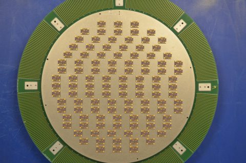
To meet this challenge, we introduced the TrueScale Matrix 300mm full-wafer probe card which enables test cost reduction by maximizing test throughput and delivering a zero-defect probing process. Amy touched on four capabilities in the article:
1. It maximizes the probing area to cover the entire 300mm wafer, which provides opportunities to test as many dies as the tester channel allows, without any area limitation. Most alternate probe cards are limited to a probing area of 100mm to 150mm.
2. It has a proprietary touchdown optimization tool that allows you to create inventive patterns to maximize throughput. The “rainbow” pattern provides lower touchdowns compared to a rectangular probe card’s “solid wall” pattern. Simply put, a circular probing pattern is more efficient for a round wafer.
3. Our proprietary TRE™ (Test Resource Enhancement) technology provides a boost to wafer test throughput. The TRE option can intelligently split a single tester resource to test multiple dies, without compromising test quality.
4. It delivers ultra-low force design to support zero-defect manufacturing. The probe is designed with ultra-low force—less than 2 grams probe force per probe—to ensure that the active circuitry below the probing pad is undisturbed after multiple probing insertions at the same pad location.
Validated by key automotive manufacturers and deployed to various tester platforms (T2000, V93K DD, J750), the TrueScale Matrix 300mm wafer probe card is helping manufacturers to meet the zero-defect challenge. For details, download Hirofumi Nagata and Alan Liao’s presentation from SWTest Asia – Ultra High Temperature Probe Card Solution for Automotive IC Testing.