Following the recent release of some breakthrough new Silicon Photonics (SiPh) probe advancements for the CM300xi probe station, we wanted to circle back and dive into some detail. We previously showcased some highlights of the OptoVue Pro™, which enables optical positioner calibrations to be performed in-situ, without the removal of the current wafer being tested, resulting in faster time to data. Here, we’ll dive into the new edge coupling efficiencies for high bandwidth.
For Horizontal Die-Level Edge Coupling
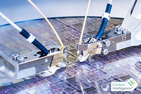
The best coupling efficiency for high bandwidth applications is achieved by getting fibers/arrays as close as possible to the exposed waveguide facet(s) through horizontal die-level edge coupling. True edge coupling enables close simulation of real-world conditions with device performance closest to the final application.
We provide the only solution on the market that enables advanced automated alignment for horizontal die-level edge coupling, deploying exclusive automated fiber-to-facet alignment techniques and reducing the risk of damaging fibers to a minimum with collision avoidance technology.
Unique software algorithms like AlignOpticalProbes3D (see below) enable optimizing the fiber-to-facet gap versus maximum coupled power at both the input and output.
No other solution available enables you to get the positioning hardware calibrated in the YZ plane and ready to perform edge coupled optical optimizations.
For Wafer-Level Edge Coupling
Wafer-level edge coupling is now possible with a new innovative combination of hardware and software features to align and optimize fibers/ arrays in a wafer-level trench.
A suite of software alignment algorithms enables YZ optimization scans in a wafer trench while tapered lensed fiber holders provide a low approach angle relative to the wafer surface. This enables alignment of the probe in the trench as close as possible to the facets, minimizing coupling losses with minimal trench dimensions.
The solution means easy setup even for less experienced users, repeatable measurement results due to unique fiber-to-facet gap alignment technology, and reduced risk of damaging fibers with collision avoidance technology.
Here are four key features of our leading-edge alignment solutions that are now available:
1. Measure3DCoupling – performs successive area scans and stepping moves along the coupling axis, constructing a 3D image of power coupling. Useful for multiple purposes such as detecting fiber damage, detecting DUT contamination, measuring the focal length of lensed fiber, etc. Applicable to both edge and vertical coupling.
2. AlignOpticalProbesEdge – executes a vision-based gap alignment on multiple selected probes and then performs YZ area scans while recentering as necessary.
3. AlignOpticalProbes3D – searches for the optimum gap for both input and output fibers that results in the maximum coupled power.
4. AlignOpticalProbeGap – executes a vision-based gap alignment on a single probe in XY, moves to probe height in Z and readies for a YZ area scan.
For more information on these and other new features for Silicon Photonics device measurements, check out the press release announcement or download the brochure.