Power Consumption
on the Rise
Greater demand for energy efficiency in systems, cars, consumer appliances, portable electronics, and new connections to the Internet of Things are continuing to drive the advancement of power semiconductor devices, with year on year record-high level demand.
As a result, companies and foundries around the world are increasing test capacity in R&D, high-performance device production and general high-volume manufacturing. Next generation power devices are rapidly being developed to bring down end-user device costs and support a wide range of growing application performance needs.
According to industry reports, 68% of power devices in power electronics were for low voltage applications (<900 V) in the year 2017. The remaining segment of power devices (32%), where significant growth is occurring, is split by voltage as follows: medium (1 – 1.9 kV), high (2 – 3.3 kV) and very high (>3.3 kV) voltage applications.*
Electric vehicles and transportation are two areas where the use of power semiconductor devices/ modules is expanding. Higher current handling (200 – 400 A) and higher voltages (3.3 – 10 kV) are required at elevated temperatures (300 – 400° C) to meet new reliability and performance specifications. This requires extensive R&D device characterization and manufacturing test development.
A key challenge engineers face, is testing on-wafer instead of in-package. FormFactor is already playing a significant role in on-wafer power semiconductor test.
New Materials for a New Age
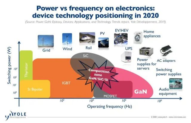
Currently, 98.7% of power semiconductors are manufactured using silicon substrate material. However, there is a migration from Si to wide band gap substrate materials (GaN and SiC), that promises significant power semiconductor performance gains. In the next four to five years, the use of these materials is projected to grow by up to 3.9% ($1.7 billion).*
In general, SiC and GaN high power semiconductors can operate at higher temperatures and with greater efficiency. Specifically, research and development for GaN is interesting for faster switching and SiC for high temperature applications. Devices that can support higher temperatures allow increased reliability, i.e. for automotive electric vehicle. Devices that can support faster switching enable lower energy loss. Both, GaN and SiC based devices can be smaller than Si based devices which results in smaller packaging into consumer products.
While on-wafer testing methodologies for GaN and SiC power semiconductors (lateral and vertical structures) are similar for Si devices, expanded test capabilities are needed for these newer wide band gap devices.
* Source: Yole Développement, 2020
When Test Complexity Must be Simplified

Power semiconductor devices are typically used as switches or rectifiers in power electronic circuits. These are commonly referred to as power device, power ICs, and power modules. Some common power devices include power diode, power MOSFETs, and IGBTs (Insulated Gate Bipolar Transistors).
When engineers and designers are developing next generation devices they need to collect key parameters during testing. These include the following for power semiconductors:
- Breakdown voltage
- Low leakage @ high voltage
- On-resistance RDS (on)* for high current
- Rise and fall times for switching
- Safe-operating area (thermal dissipation and “latch-up”)
- Thermal resistance
However, when testing Si and advanced GaN/ SiC devices on-wafer instead of in-package, R&D engineers and test operators are faced with some major challenges to collect high accuracy data. These include the need for probe and system anti-arcing at high voltage, low resistance probe and wafer contacts for high current, and special handling for thinned wafers. Simultaneously, the need for “fast time to accurate data“ requires quick and easy setup of complex high power test configurations. And, with operator and device safety in mind.
*”RDS (on)” stands for “drain-source on resistance” in a MOSFET.
Challenges
Anti-arcing for high voltages
Typically, when measuring high voltages on-wafer there will be electrical discharge (arcing) between probe needles. This also occurs between the DUT (device under test) and adjacent devices (vertical layouts) or other test pads (lateral layouts). In addition, arcing can occur between the wafer chuck and the surrounding probe station at voltages above 1000 V.
Low contact resistance of the probe to device
Another key challenge to achieving accurate high current measurements is to keep the contact resistance of the probe to device as low as possible. This will ensure that the full performance of the device can be measured on-wafer with full correlation to in-package performance. This leads to significantly lower costs using known good die for final end-application power modules.
Low contact and thermal resistance, with uniformity between wafer and chuck
To get accurate data for every device on the wafer, it is important to have uniform physical contact between the wafer backside and the chuck top surface. Firstly, this reduces thermal errors by ensuring full device-generated heat is distributed away from each device, no-matter the device location on the wafer. And secondly, for vertical devices (such as IGBT’s) where the chuck functions as one of the electrical contacts, this enables ultra-low contact resistance – a critical need in overcoming resistance errors for non-kelvin testing of RDS(on). Only when both challenges are solved can each device’s maximum performance be seen in testing data.
Accurate device models for Circuit Designers
A challenge for device characterization engineers is to measure both high voltage/high current AND accurate low leakage performance to create a complete device model. This will help circuit designers to optimize their power IC designs for maximum commercial value. Balancing high voltage/current switching versus device power consumption when not operating (off-state leakage) is a key focus of this work.
FormFactor has solved these measurement challenges working together with key device manufacturers and continues to lead the industry with guaranteed solutions for accurate data and reduced cost of test.
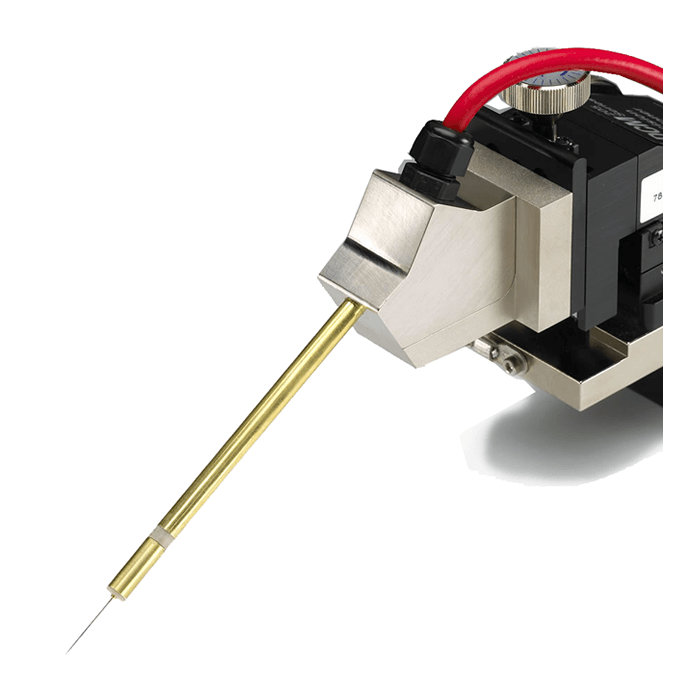
") High-current Probes |
 |
 High-voltage/current Triax Chuck |
 High-voltage Probes |

High-voltage/current Chuck Port |
|
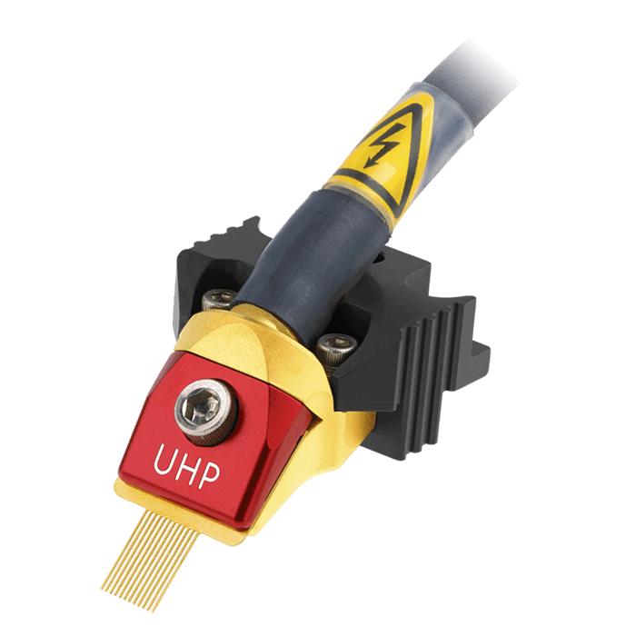
 Ultra High-power Probes |

Connection Packages |
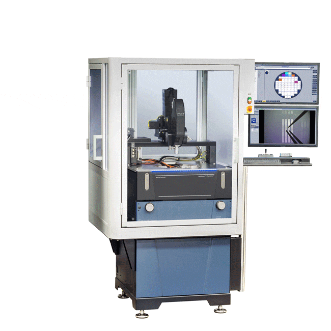
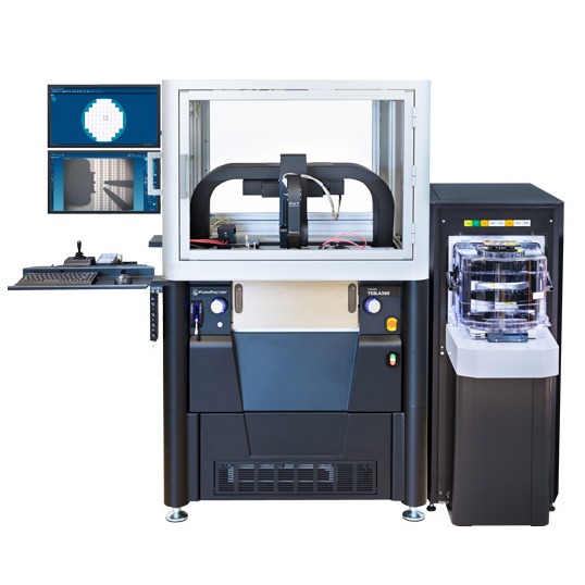
TESLA200 - 200mm High Power Probe System
| The TESLA200 Advanced On-Wafer Power Semiconductor Probe System is an integrated high-power test solution that enables collection of accurate high voltage and high current measurement data, with complete operator safety. |