Products
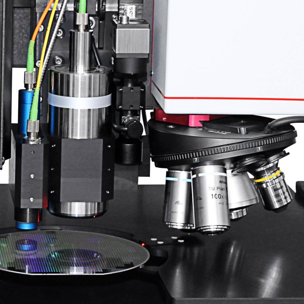
FRT surface metrology tools are used for production, development, and quality control. Based on the design and construction of these multi-sensor devices, these tools can be used for a wide range of wafer and non-wafer applications.
Fully Automated Wafer Metrology
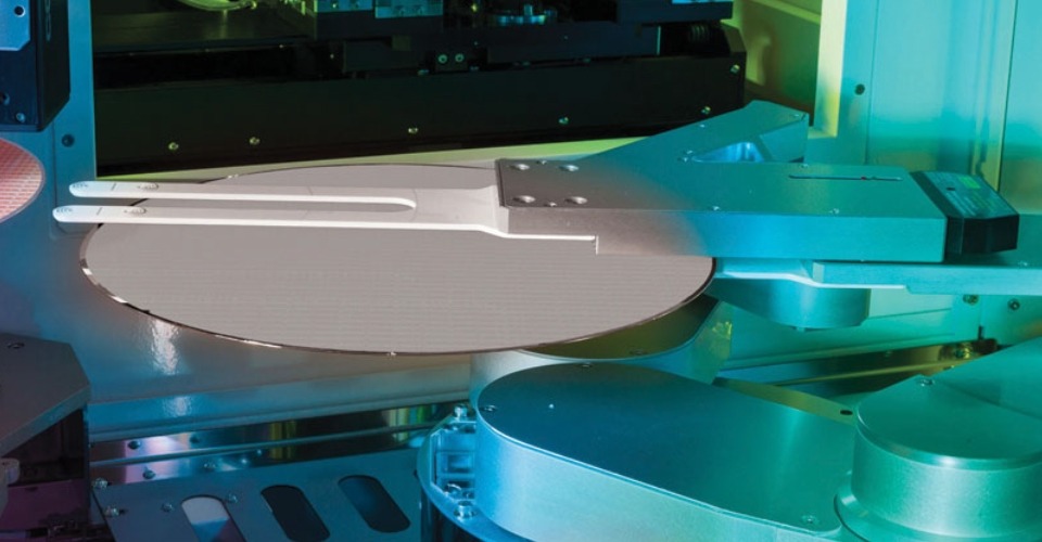
The standard fully automated wafer metrology tools combine the capabilities of the worldwide established 300 mm metrology station, with a wafer handling system within an Equipment Front End Module (EFEM)
Learn More >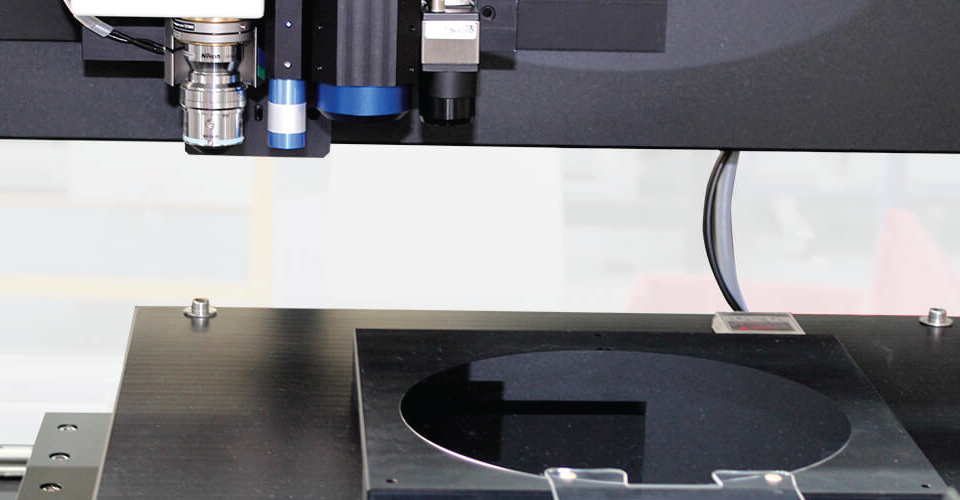
Semi-automated with MHU
The metrology tool with material handling unit (fully automated handling, manual cassette placement) is developed especially for the semiconductor, MEMS, sapphire, and LED industries.
Learn More >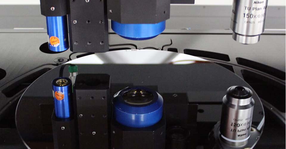
Manual Metrology
High-precision optical surface metrology tools for the characterization of various functional and/or technical surfaces - fast, efficient, non-destructive. Maximum flexibility is provided by the multi-sensor technology, developed by FRT Metrology.
Learn More >