Amazing MEMS
Innovative technology at the heart of advanced wafer probe cards enables wafer test
MEMS: Micro-Electro-Mechanical Systems
The genius of MEMS (Micro-Electro-Mechanical Systems) is at the heart of advanced wafer probe cards, accounting for ~75% of the world’s advanced probe card market. MEMS technology provides a way to manufacture the probes, which contact the I/Os and power connections on ICs at micron-level perfection. The precision of MEMS probes makes it ideal to support fine-pitch and high-pin count requirements of the leading-edge semiconductor process nodes and advanced packaging. But not all MEMS probes are created equal. Find out how FormFactor composite-metal MEMS technology is enabling a range of new ICs at the cutting edge of electronics innovations.
FormFactor MEMS probe cards are at the forefront of these innovations, addressing the challenges of advanced 2.5/3D packages, the wide temperature requirements to test ICs for the automotive industry, the emerging needs for high bandwidth and excellent signal integrity in RF applications, and reducing the cost to test thousands of DRAM memory devices in a single touchdown.

What is MEMS? In this short animated presentation, we show you how we fabricate our unique MEMS probes, the integral elements of our advanced wafer probe cards.

FormFactor MEMS Podcast Series (Episode 1): What is MEMS and How is it Used in Wafer Probe Testing?
FormFactor’s Chief Technology Officer Jarek Kister describes MEMS technology and how FormFactor uses sophisticated MEMS metallization to build millions of tiny robust electrical springs capable of testing ICs over more than a million contact cycles (touchdowns).
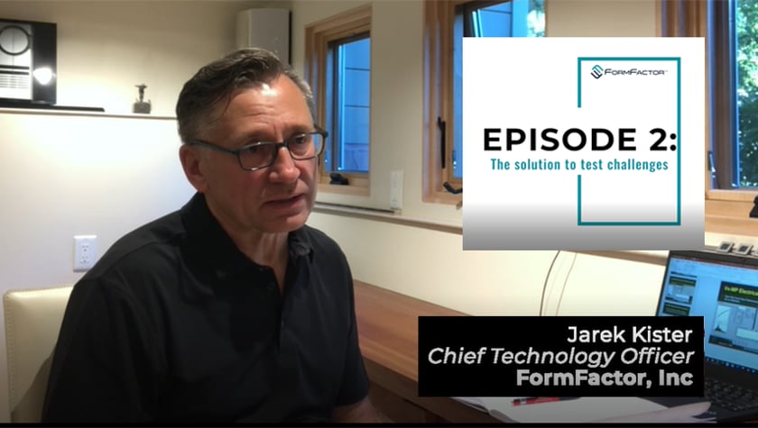
FormFactor MEMS Podcast Series (Episode 2): MEMS – The Solution to Test Challenges
FormFactor’s Chief Technology Officer Jarek Kister discusses the application of MEMS to high parallelism wafer probing and how FormFactor’s MEMS technology solves challenging microprocessor test requirements.

FormFactor MEMS Podcast Series (Episode 3): – Hybrid MEMS
FormFactor’s CTO Jarek Kister explains how the company’s Hybrid MEMS technology enables engineers to balance contact force, high current carrying capability and ultra-fine pitch to optimize for advanced wafer probe requirements.
MEMS - Technical Papers
Next Generation KGD Memory Test Achieved Wafer Level Speed Beyond 3GHz | Lee
Presented at TestVision 2021
Recent industry wide adoption of heterogeneous integrated system enabled by 2.5D and 3D advanced packaging technology is driving up the demand for known-good-die (KGD) and known-good-stacked-die (KGSD). Coupled with the advancement on DRAM and High Bandwidth Memory (HBM) native speed capability, the latest memory is running beyond 2GHz (4Gbps) which is pushing the limit on existing ATE testers. Recent joint effort between SK Hynix, FormFactor, and Advantest successfully demonstrated that beyond 3GHz is achievable. This session discusses the design challenges overcame in this collaboration from a system level signal integrity and power delivery perspective.
Digital Revolution: PAM4 Wafer Test | Raschko
Presented at TestVision 2021
As data rates continue to increase, the difficulty of increasing clock rates for improved bitstreams becomes more challenging with ever-increasing loss. As of today, Non-Return-to-Zero (NRZ) is the standard for digital encoding, but this begins to run into problems with loss and the collapse of the digital eye beyond 40 Gbps. To counter this, Pulse Amplitude Modulation 4-Level (PAM4) is beginning to emerge in digital communications which allows for the same fundamental frequency to be used as NRZ while doubling the data rate by introducing two additional amplitude levels to the traditional 2-level encoding. This paper will address the implications of this change for wafer test and will explore the sensitivity of PAM4 to different types of loss along with how this loss can be countered in the probe card.
5G: The Phanerozoic Eon of Parallelism | Bock
Presented at TestVision 2021
5G has been pushing on wafer test of several years now and the test cell is evolving to more complex systems. Same as the change to multicellular life during the Phanerozoic Eon, we are seeing a concerted change to multi-DUT testing with 5G parts in order to improve the output from manufacturing wafer test. Now, 5G is in the middle of ramp, with more handsets being released with 5G FR2 chipsets being released. Current estimates put up to a 150.7% CAGR increase in the number of devices with 5G from now until 2024. This growth requires a subsequent increase in the wafer test capability in the manufacturing flow to provide Known Good Die (KGD) in a reasonable cost of test. There are multiple ways to increase the volume and minimize cost of test. Some of these include more test cells, but buying more testers is can become cost prohibitive. Another strategy is to provide more test parallelism with upgraded testers that have mW frequency capability with a low number of channels in the tester, but resources are extended by using switches and other types of channel count increase. Another method is to use wafer loopback test, but that reduces the test visibility due to the signals never getting back to the tester. All of these have advantages and drawbacks. We will discuss multiple ways to do this as well as discuss the Cost of Ownership Implications.
The Digital Revolution: NRZ to PAM4 | Bock, Raschko
Best Overall Presentation - SWTest 2021
With increasing demand to process more data and pass large amounts of data through servers, cellular devices, and even within the computer for the highest performing video cards, the need for more complex digital processing is becoming greater than ever. In this presentation, Daniel Bock and David Raschko will show some of the impacts of NRZ compared to PAM4 on wafer test through example probe cards and describe the changing test requirements.
Next Generation KGD Memory Test Achieved Wafer Level Speed Beyond 3 GHz/6 Gbps | Liao
Presented at SWTest 2021
Recent industry wide adoption of heterogeneous integrated system enabled by 2.5D and 3D advanced packaging technology is driving up the demand for known-good-die. Coupled with the advancement on DRAM and High Bandwidth Memory (HBM) native speed capability, the latest memory is running beyond 2 GHz (4 Gbps) which is pushing the limit on existing ATE testers. Recent joint effort between SK Hynix, FormFactor and Advantest successfully demonstrated that beyond 3 GHz is achievable. This session discusses the design challenges overcame in this collaboration from a system level signal integrity and power delivery perspective.
Next Generation SmartMatrix Probe Card Technology Enables 3000-Parallelism 1TD Test for 1Z DRAM Process Node | Ceremuga
Presented at SWTest 2021
The DRAM technology process node continues to shrink, driven by the demand to increase bit density and reduce memory device cost. With the recent accelerated transition from the 1Y to 1Z process node, die count per wafer is increasing rapidly. Wafer sort throughput must advance to achieve the target cost without adding significant capital expenditure to the existing test floor. Samsung and FormFactor have been working together, and successfully developed and qualified the next generation DRAM probe card that leverages FormFactor’s ATRE technology for 3000-parallelism and beyond. FormFactor’s SmartMatrix 3000XP probe card enables remarkable high-parallelism test throughput by extending ATE tester resource sharing up to X32. This session discusses the key technology enablers of the SmartMatrix 3000XP product architecture, and the design challenges overcame during this successful collaboration.
Challenges of Expanding Large Area Active Array for Fine Pitch Vertical Probe Cards | Harker, Desta
Best Data Presentation - SWTest 2021
Semiconductor manufacturers are on a relentless drive to reduce the total cost of test at sort. A major contributor to reducing cost of test is increasing simulations Device Under Test which requires a subsequent increase in the probe card active area. FormFactor has developed a new probe card architecture to address the challenges of fine pitch, high CCC, and high temperature range for wire bond probing applications.