Contact Us

Two popular uses for semiconductors and compound semiconductor materials in the optical device industry are the applications of LED and CMOS image sensor manufacturing. LEDs convert electricity to light by way of semiconductor materials and CMOS image sensors convert light passed through a lens to digital information. The two applications have broadly changed the home and commercial lighting industries, and revolutionized the camera industry in the conversion from analog to digital image capture.
CMOS Image Sensors (CIS)

A CMOS (Complementary Metal Oxide Semiconductor) image sensor converts photons into electrical charges to create digital images. This optical technology is used in a variety of high-speed imaging applications, including smartphones, PCs, tablets, and automobiles. As smartphone manufacturers continue to increase the quality of their cameras, CMOS technology is expected to advance and rise in adoption. With sensitivities to light fixed pattern noise and particles, CIS devices have unique testing requirements to ensure their optimal operation.

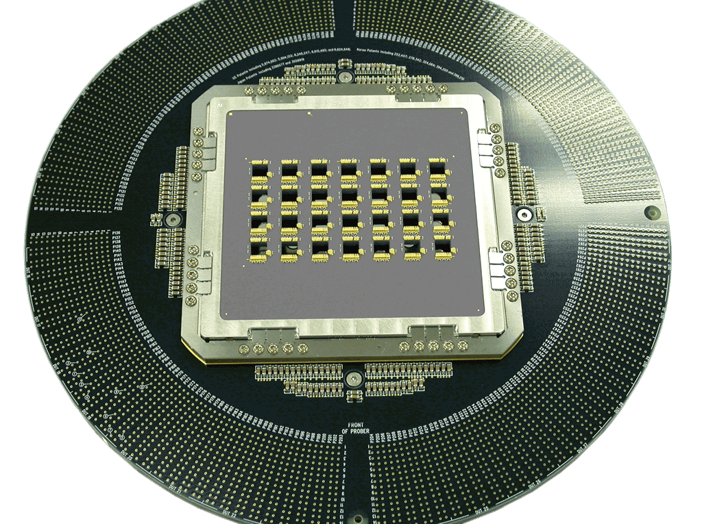
FormFactor’s Hikari probe card solution delivers excellent light uniformity, low power noise within the DUT and across the array, with minimal pad damage. These capabilities allow CMOS image sensor manufacturers to reduce test time and maximize yields.

Hikari offers a customized lens module with options for split pixels and diffusers. Hikari’s optimized array configuration enables customers to achieve the fewest touchdowns at the lowest parallelism. At x64 arrays, Hikari can provide high frequency lines (LVDS) at up to 3.5 Gbps. With fewer touchdowns, re-sorts, and frames required for image capture, Hikari delivers a high-throughput test solution for CMOS image sensors.

Modern devices with high pixel count and small pixel sizes are more prone to particle defects, which can cause false failures during test. Leveraging FormFactor’s 3D MEMS MicroSpring® technology, the Hikari platform ensures consistent and small scrub marks for minimal pad damage and particle debris. Hikari is also capable of testing at a wide temperature range to meet automotive image sensor requirements.