Computing, Data Centers and Quantum — from Lab to Fab
To meet the world’s persistent demand for high data throughput at minimum energy levels, the semiconductor industry has aggressively pursued the development of new technologies and the refinement of existing ones for processing and storing data. FormFactor is deeply involved in this development, as virtually all these devices must be tested at the wafer-level as they move from the lab to fab.
Integrated circuits (ICs) with feature sizes as small as 3 nm promise to combine high throughput with optimal energy efficiency in high performance computing (HPC) settings, like AI and data centers. We’re already delivering the industry’s most-trusted, advanced wafer probing techniques for both R&D and high-volume production of leading-edge CMOS technologies.
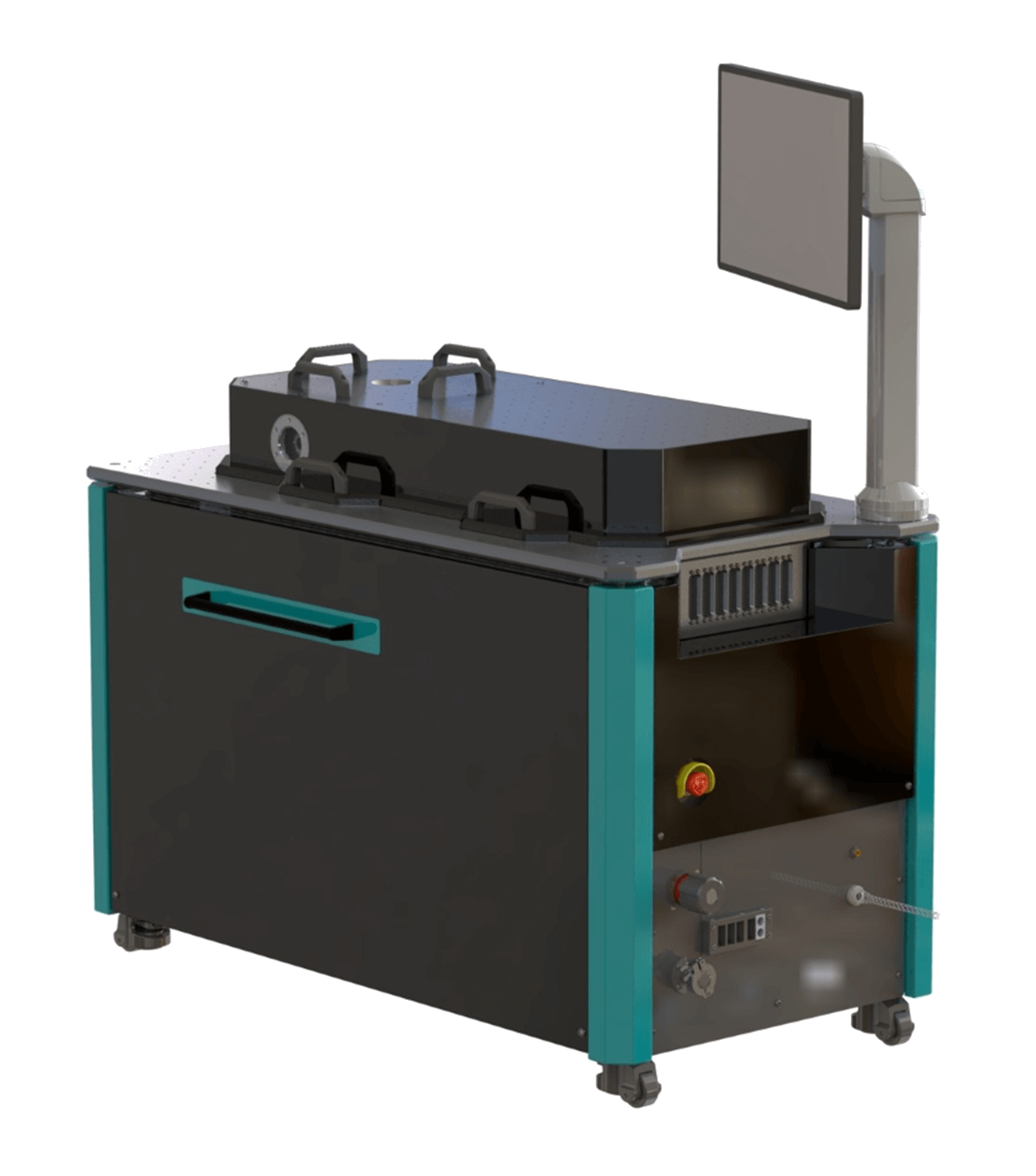
Quantum computing, once only theoretical, is moving steadily toward practical realization. Quantum devices operate at extremely low temperatures provided by our cryogenic probing systems.
FormFactor enables the data generation industry from lab to fab. As a leader in test and measurement our products and expertise are used in the following applications:
| Research / Development |
High Volume Engineering |
Niche Production |
High Volume Manufacturing |
|
|---|---|---|---|---|
| Quantum Computing | ||||
| Silicon Photonics | ||||
| Advanced Node | ||||
| AI Processors | ||||
| CPU / GPU / Logic | ||||
| Memory |
- Quantum Computing
- Research / Development
- High Volume Engineering
- Niche Production
- High Volume Manufacturing
- Silicon Photonics
- Research / Development
- High Volume Engineering
- Niche Production
- High Volume Manufacturing
- Advanced Node
- Research / Development
- High Volume Engineering
- Niche Production
- High Volume Manufacturing
- AI Processors
- Research / Development
- High Volume Engineering
- Niche Production
- High Volume Manufacturing
- CPU / GPU / Logic
- Research / Development
- High Volume Engineering
- Niche Production
- High Volume Manufacturing
- Memory
- Research / Development
- High Volume Engineering
- Niche Production
- High Volume Manufacturing
What's New
-
FormFactor Introduces Rapid Cooling Probe System for Quantum Device Testing
The IQ2000™ Cryogenic Chip Scale Probe System tests 10X more devices at 4 Kelvin
Published in Press Releases
-
FormFactor Named One of THE BEST Suppliers in the Semiconductor Industry for Tenth Consecutive Year
FormFactor receives a five-star rating in Annual TechInsights VLSI research customer satisfaction survey.
Published in Press Releases
-
Silicon Photonics (SiPh) Moving to Production
Learn about the ongoing development that is advancing photonics testing towards broad volume production.
Published in Blog
Quantum/Superconducting
Quantum computers stand poised to deliver dramatic breakthroughs in any number of scientific and engineering fields. Personalized drugs, pinpoint weather predictions, better batteries and super-secure encryption all fall within the realm of possibility, along with many other applications.
In parallel, another category of machines called superconducting computers promises to elevate conventional computing to the so-called exascale level, where they will deliver formidable processing speed at only one tenth the power of present technology.
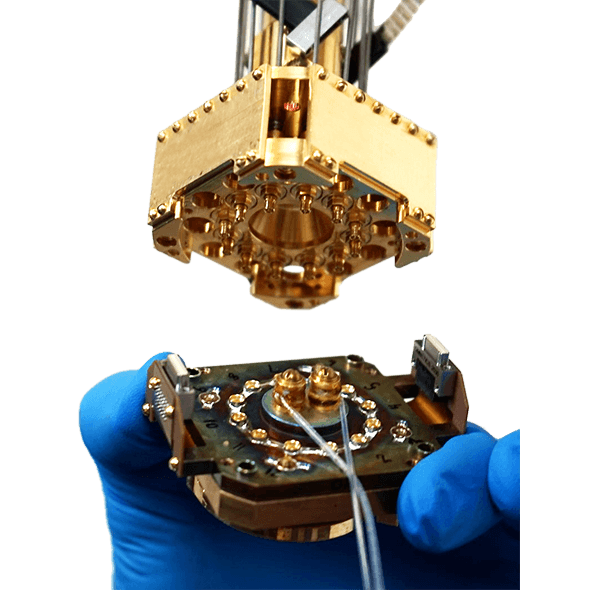
Both quantum and superconducting computers share a common requirement on their journey from the lab to fabrication: they can only function at ultra-low temperatures approaching absolute zero. FormFactor has taken aggressive steps to address this challenge by providing cryogenic environment systems, offering a suite of products including sub-10 mK dilution refrigerators, sub-100 mK cryostats, cryogenic chip-scale and wafer-scale probers, engineering probes, and probe cards.
Learn about cryogenic test applicationsFeatured Products
Learn More
-
Superconducting and Spin Qubit Pre-Screening Brochure
Integrated measurement solutions with Keysight and SeeQC for advanced quantum development.
Published in Technical Papers
-
Webinar: Quantum and CryoCMOS: Enabling the Future of Computing with Advanced Test & Measurement Tools
Learn more about cryogenic wafer probing on SFQ circuits, enabling the acquisition of statistical datasets in hours—a process that would otherwise take weeks or months.
Published in Webinars
Silicon Photonics
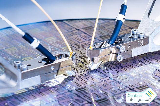
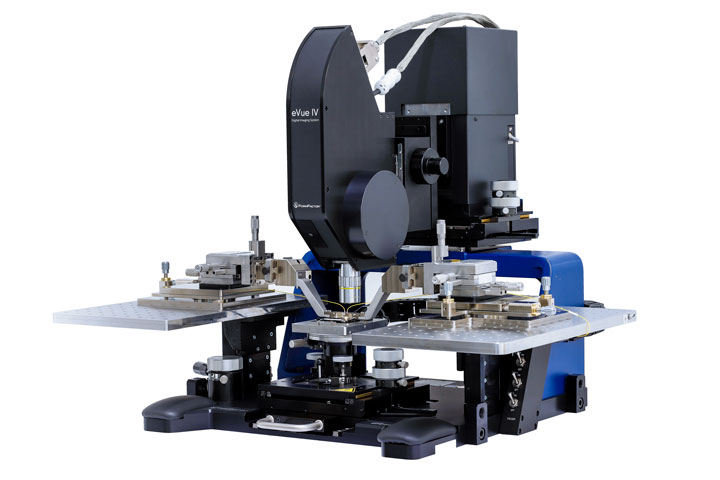
Silicon photonics (SiPh) holds the potential for spectacular gains in speed and power efficiency. The first wave of the SiPh revolution stands poised to roll over data centers around the world with optical interconnects that breach the self-heating barriers set by copper wire. Bandwidths of a terabit per second now come within practical reach. Additionally, new applications such as glucose monitoring and blood typing are evolving around silicon photonics.
FormFactor already plays a significant role in the implementation of silicon photonics technology. This illustrates how we participate in solving the challenges of wafer test long before a new technology goes into mass production.
Learn more about silicon photonicsFeatured Products
Learn More
-
Silicon Photonics (SiPh) Moving to Production
Learn about the ongoing development that is advancing photonics testing towards broad volume production.
Published in Blog
-
Webinar: Pharos Vertical and Edge Coupling Low Loss SiPh Wafer Test with Fully Automated Calibration
Learn about our industry-leading SiPh coupling technology, Pharos, for edge coupling in V grooves and lowest loss coupling on grating couplers.
Published in Webinars
Artificial Intelligence Processors
Artificial Intelligence (AI), once the stuff of science fiction movies, now manifests in various forms—from personal assistants in cell phones to tailored movie recommendations and drone-based pipeline inspections, among others.
AI’s neural networks learn much like their biological counterparts, relying on examples and repetition rather than the sequential logic of standard computer programming. These networks consist of large concentrations of interconnected nodes, each representing the equivalent of a single neuron. Essentially, each node acts as an independent algorithm, exchanging data with its peers as the network gains intelligence and arrives at solutions.
In general, this process requires voluminous amounts of computing power to continually model the behavior of each node during each training cycle. This makes AI’s machine learning an ideal candidate for massive parallel processing. Massive parallelism once existed exclusively in the realm of supercomputers, but recent advances in chip technology now allow it to reside on a single IC substrate that integrates billions of transistors.
As AI continues its integration into new generations of silicon, FormFactor remains committed to providing wafer probe solutions that contribute to its development.
Learn more about artificial intelligenceFeatured Products
Learn More
-
Artificial Intelligence Comes of Age
As AI continues its migration into new generations of silicon, we’re committed to being there with wafer probe solutions that help make it possible.
Published in Technical Papers
-
Kepler and Apollo Probe Cards Meet the Challenges of Advanced AI
FormFactor has a new generation of wafer probe cards that can land on arrays of microbumps as small as 25 µm and can carry more than an amp of current without overheating and warping.
Published in Blog
CPU / GPU / Logic
The explosion of data generated by internet traffic and a myriad of other sources is demanding faster and faster server processors and artificial intelligence for real-time decision-making capability. With the decline of Moore’s Law, advanced processors now turn to next-generation advanced packaging techniques to sustain the pace of innovation demanded by HPC applications. Heterogenous integration ties processors, memory, I/O, logic, and interposers together with bumps, pillars, through-silicon vias, and other elements.
Wearables, smart phones, and Internet of Things (IOT) also drive the development of small, high performance, long battery life devices, and utilize wire bond, flip-chip, and wafer-level packaging in smaller and smaller form factors.
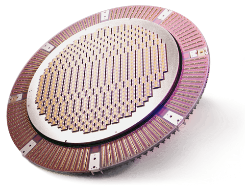
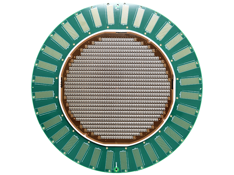
Advanced package technologies, very large and very small dies, and increasing probe pad density create new wafer probing challenges. FormFactor leads the industry in the breadth of advanced, MEMS-based probe card solutions to these challenges, able to test thousands of dies simultaneously, with hundreds of thousands of parallel probes, and even probing directly on 3D contact elements.
Learn more about logic/SOC
Featured Products
Learn More
-
Current Carrying Capacity Maximization in Probe Cards and the Path to An Unburnable Probe
This paper highlights several techniques that can be utilized in the probe card to maximize CCC and achieve an effective CCC of >2.5 A in a probe card at an 80 um minimum pitch.
Published in Technical Papers
-
Advancing Probe Card Parallelism for SOC Devices
: In order to reduce the cost of test for automotive devices, Infineon worked with FormFactor to implement the production proven TrueScale Matrix platform for the V9300 direct dock tester.
Published in Technical Papers
Memory
Our interconnected society generates exponentially increasing amounts of data, with multiple zettabytes (each zettabyte is approximately 10^21 bytes) per year in internet traffic. Data centers, mobile devices such as cellphones, smart IoT devices, and more, all need more DRAM and flash memory than ever before. Higher-density, faster flash and DRAM memory such as HBM (high bandwidth memory) leverage advanced packaging techniques, sometimes stacking over a hundred die in a single IC package.
As the memory IC market continues to advance and expand, semiconductor manufacturers face the complex challenges of high parallelism and full-wafer contact testing. FormFactor’s range of high-performance wafer test solutions help chip suppliers achieve yield optimization, lower cost of test, and faster time-to-market for today’s advanced memory devices.
Learn More about memory
Featured Products
Learn More
-
Next Generation SmartMatrix Probe Card Technology Enables 3000-Parallelism 1TD Test for 1Z DRAM Process Node
Samsung and FormFactor have been working together, and successfully developed and qualified the next generation DRAM probe card that leverages FormFactor’s ATRE technology for 3000-parallelism and beyond.
Published in Technical Papers
-
Next Generation KGD Memory Test Achieved Wafer Level Speed Beyond 3 GHz/6 Gbps
Recent joint effort between SK Hynix, FormFactor and Advantest successfully demonstrated that beyond 3 GHz is achievable.
Published in Technical Papers