Sharing Expertise—
Pushing Technology Boundaries Together
FormFactor draws on its deep understanding of semiconductor test and measurement to form highly productive relationships with industry and technology leaders.
By sharing expertise, all participants benefit: customers build better products, instrument makers advance their technology, fab equipment makers improve their process, and we remain at the forefront of wafer probe technology. This broad collaboration advances simultaneously on multiple fronts. Our R&D engineers work through novel challenges presented by our customers as they move into uncharted technological territories. Our field applications teams respond with creativity and resourcefulness. Our leadership reaches out to other organizations in setting standards and policies. In the end, we understand that pushing the boundaries of both digital and analog technology is a team effort, one that requires all of us to unite in a common effort.
Putting 30 Years of Semiconductor Test
Experience to Work for Customers
The escalating pace of technological progress makes each node change, new wafer material, or chip design somewhat of a voyage into the unknown. To understand the resulting implications across the entire design to test continuum, FormFactor works closely with customers during the development cycle, sharing knowledge and expertise. We roll up our sleeves and work directly with each engineering team to deliver timely solutions, both in the lab and on the production floor.
In the process, we draw upon over 30 years of cumulative engineering experience covering virtually every aspect of semiconductor design and test. Our in-house research and development team utilizes its vast store of information and experience to directly address the wide array of wafer probing issues confronting our customers on a daily basis. At the same time, we leverage a strong network of close relationships with the industry’s foremost technology partners to solve specific applications issues.
From chips operating in the frigid vacuum of outer space to the extreme heat in automobile engines, we’re dedicated to delivering fresh and innovative wafer probe solutions that fully leverage what we’ve learned. What follows are just few examples of the diverse engineering scenarios we routinely encounter.
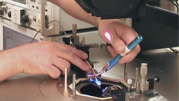
How We Measure Up
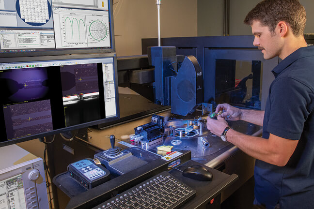
Our goal is to deliver the best possible signal from the wafer surface to precision instruments. To meet this goal, we collaborate with instrumentation providers on a regular basis to optimize performance and accuracy.
Device characterization represents one broad area of collaboration. Understanding the interplay between IC performance and variations in its fabrication process is essential to building competitive products. It plays a critical role in constructing accurate simulation models, and in yield improvement and quality control. It also demands the generation of substantial volumes of data, which in turn dictates maximum automation of wafer handling and probing during the measurement process—all with no compromise in precision and accuracy.
Our latest generation of probe stations, integrated with the highest quality instrumentation and software, meet this challenge on a variety of fronts. DC, RF/microwave and high-power probing are fully supported up into the Terahertz (THz) range and Kelvin (kV) levels; thermal ranges extend from -60°C to +300°C; and multiple levels of automation are available that extend from lab to fab. Additionally, specialized FormFactor probe stations can provide solutions for extreme temperature requirements.
One specialized field of collaboration centers on the characterization of devices operating in the RF range, which employs S-Parameter testing using sophisticated network analyzers. In response, our probe systems fully support multi-port testing to 100’s of GHz and beyond, with highly automated calibration and maximum noise shielding.
Probing the Upper Limits
Terahertz (THz) technology, once the province of exotic scientific applications, has now moved into mainstream markets including imaging and communications. For signals in the THz range (300 GHz to 3 THz), waveguides come into play as a means of propagating electromagnetic waves from one circuit node to another. These hollow, rectangular metal structures, whose dimensions determine the precise nature of the RF signal being propagated, represent a radical departure from conventional coaxial cable transmission and require highly specialized wafer probing technology.
In response to the escalating need for high-performance THz solutions, we have partnered with Dominion MicroProbes, which employs unique micromachining technology to fabricate RF wafer probes capable of delivering accurate test results at extreme frequencies. By integrating these advanced probes into many of our wafer probe systems, such as the Summit probe station, we deliver fully supported and guaranteed solutions to device designers working in the THz realm.
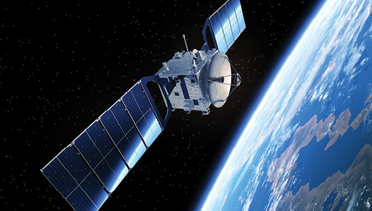
Extreme Environments Call for Extraordinary Test Solutions
The far reaches of outer space present the ultimate challenge to device manufacturers. Operating temperatures can plunge to just a few Kelvin. At the same time, powerful magnetic fluxes can profoundly influence the behavior of semiconductor materials.
In response, researchers have developed a new generation of device materials that meet the extraordinary demands of outer space and other extreme environments. One of the principal challenges during this effort is accurate test and measurement: How do you duplicate these extreme conditions in the lab? How do you maintain the integrity of your probing operations in this kind of environment, where even the heat of the probe can influence the results?
To find the answers, we formed a partnership through our MeasureOne™ program with Lake Shore Cryogenics, which specializes in device characterization under extreme temperatures and magnetic conditions. Lake Shore provides high-precision, micro-manipulated probe stages that allow scientists and engineers to perform a broad range of tests with the highest possible confidence. When combined with our probe stations, this partnership gives customers a continuous device characterization path all the way from the earliest investigations through to process control during mass production.
Scaling the Heights of 3D Packaging
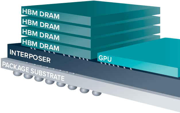
One prime driver of today’s system integration and scaling is 2.5D/3D chip packaging, which makes maximum use of available real estate by vertically stacking multiple layers of circuitry in a single package. A prime example is high bandwidth memory (HBM), which is rapidly growing to enable next-generation supercomputers, artificial intelligence (AI) and graphics systems.
HBM stacks multiple layers of DRAM die atop each other and uses fine-pitch silicon interposers to interconnect them with a GPU or CPU subsystem. This tight physical proximity on a single substrate maximizes both performance and integration. However, it also creates some advanced testing challenges – where to test to ensure the quality of the final stack at a reasonable cost? The ultimate solution can involve a combination of products to achieve optimal yield while achieving the lowest cost of test. In this case, the solution involved three elements: one type of probe card for massive parallel testing of the DRAM on sacrificial test access pads, and a second type for direct access probing on the singulated die or stack with grid arrays of microbumps of 25μm diameter for full functional test, and a third type to test the quality of silicon interposers to ensure TSV connectivity for critical I/Os. Working with HBM design engineers from the conceptual stage, we are able to anticipate the complex technical and economical requirements posed by this real-world production test challenge.
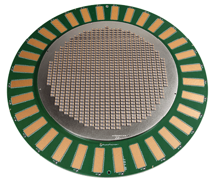
FormFactor also recently participated in a demonstration project that used our fully automated CM300 probe station fitted with our Pyramid® RBI probe card to probe on 300mm wafers, containing an array of thousands of microbumps at a pitch of 40μm. The results authenticated an accurate, cost-effective solution to the challenge of 3D wafer packaging in the engineering development environment. The relevance of this new tool was underscored by its winning the 2017 National Instruments Engineering Impact Award in Austin, Texas.