Cascade
High Current Probe
Test power devices on wafer with high-performance and low-contact resistance on smaller pads
Test power devices on wafer with high-performance and low-contact resistance on smaller pads
Looking for customer support? Ready to learn more about our products and services?
Contact Sales TodayReceive product updates and event notifications
Subscribe to Our Newsletter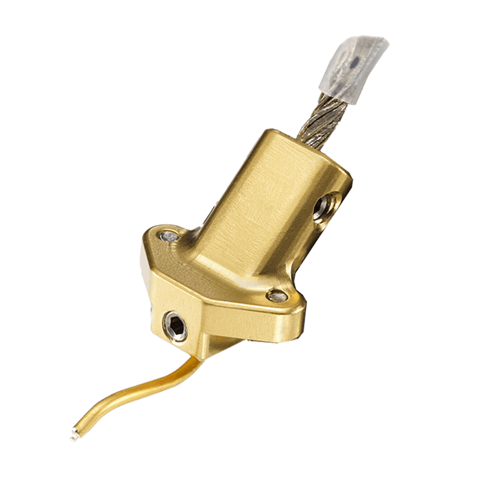
Designed specifically for testing power devices on wafer, the HCP probe reduces probe and device destruction at high currents by minimizing contact resistance at the wafer-to-probe interface to prevent device heating at the tip. The innovative multi-finger design distributes the current over multiple contact points at the tip and is joined by a single heatsink which pulls heat from the probe tip.
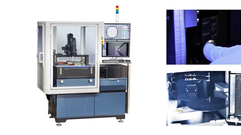
TESLA200 - 200mm High Power Probe System
The TESLA200 Advanced On-Wafer Power Semiconductor Probe System is an integrated high-power test solution that enables collection of accurate high voltage and high current measurement data, with complete operator safety.
Receive product updates and event notifications
Subscribe to Our Newsletter