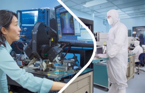
Production teams are faced with a ton of pressure these days to deliver products that are without flaw, produced quickly, and done so at the lowest possible cost. Ultimately their success comes down to how products are tested, throughout the flow of development and through the manufacturing process. Extracting data points and analyzing them throughout the semiconductor testing process begins before the first wafer is fabricated and continues all the way through final packaging, and each phase of the process produces information that is vital to successive phases.
Two relatively new IC technologies, high-bandwidth memory and silicon photonics, illustrate how we participate in moving an emerging technology from lab to fab with maximum efficiency.
High-Bandwidth Memory (HBM)
HBM stacks multiple layers of DRAM die atop each other and uses silicon interposer and copper pillars and vias to interconnect them with a GPU or CPU subsystem. This tight physical proximity on a single substrate maximizes both performance and integration. However, it also creates some advanced testing challenges. Working with HBM design engineers at the conceptual stage, we are able to anticipate the complex technical and economical requirements posed by production test. The ultimate solution can involve a combination of products to achieve optimal yield while achieving the lowest cost of test. In this case, the solution involved three elements: one type of probe card for massive parallel testing of the DRAM on sacrificial test access pads between micro-bumps, and a second type for testing the singulated die or stack with grid arrays of micro-bumps of 25 µm diameter for full functional test, and a third type to test the quality of silicon interposers to ensure TSV (through silicon via) connectivity for critical I/Os. We help our customers when they are ready for testing, and their HBM products are ready to enter the market in volume.
Silicon Photonics (SiPh)
Silicon photonics (SiPh) is an example of a technology that is both in the lab and entering the early stages of production. By fabricating optical devices in CMOS, SiPh can enable the economies of scale needed for data centers to meet ever increasing bandwidth demands while reducing power consumption and heat dissipation. Additional promising technologies for SiPh include biological sensing, LIDAR remote sensing, quantum computing. The technology is new enough that the industry has yet to settle on an established set of test and validation methodologies. To reach this point, we are actively developing technology and techniques along with key suppliers in the instrument and positioning fields to create a standardized path from initial validation though volume manufacturing.
For more information on our lab to fab expertise, stay tuned to our blog or visit our website.