Advanced Packaging Raises the Bar for Wafer Test
As companies explore advanced packaging techniques, their search leads them to seek out cost effective testing solutions to move to high volume production.
FormFactor is the only test and measurement company that provides solutions to help customers verify device performance and yield at every stage of system integration. FormFactor helps customers lower overall manufacturing cost and enables them to gain more intelligence and knowledge at every stage of this new process; helping them to make critical decisions regarding test strategies from the lab to the fab.
Diminishing Advantages of Moore’s Law Open the Way for 3D, Heterogeneous Design Alternatives
In times gone by, the role of wafer-level test in the production of semiconductor devices was relatively straightforward. No longer. Innovative technologies have emerged that allow multiple dies to be integrated into monolithic systems that satisfy the insatiable demand for cost-effective performance in top-end applications. Data centers, artificial intelligence, autonomous vehicles and hyper realistic graphics all demand unprecedented processing power—at a time when Moore’s Law by itself can no longer guarantee the price/performance advances seen in the past.
An innovative set of solutions to address these processing demands comes in the form of advanced packaging technologies that allow for scaling and performance gains independent of on-chip feature size. Some have already entered production, while others are under aggressive development. High Bandwidth Memory (HBM) uses 3D vertical stacking of DRAM memory to drive Nvidia’s graphics processing silicon to unprecedented levels. Fan Out Wafer Level Packaging (FOWLP), currently employed by Apple and TMSC, delivers both power savings and smaller footprints in portable devices. On the immediate horizon, Heterogeneous Integration (HI) technology, such as Intel’s system-in-package (SiP), allows a series of dies originating from different wafers to be integrated onto a single system substrate with extremely high interconnect density.
To be cost-effective, all of these packaging paradigms require highly optimized and accurate fabrication processes. In a multi-die system, a single defect in a single die or integration layer comes at considerable cost. As a result, wafer-level test now extends to multiple phases of the production process, making FormFactor a major participant in the development of advanced packaging technology. Our test and measurement solutions play a critical role in assuring quality and keeping manufacturing costs within limits.
Testing High Bandwidth Memory Presents Unprecedented Complexity
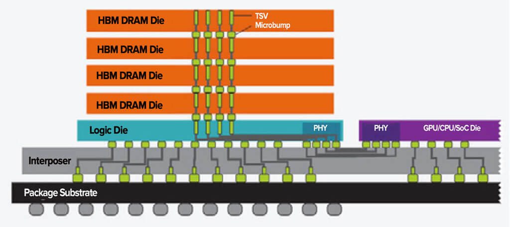
High Bandwidth Memory (HBM) provides a good case in point and demonstrates how the role of wafer-level test in the overall production flow is continually evolving. Figure 1 shows how a fully assembled system might appear. A stack of four DRAM cores is integrated with a logic layer that provides the interface to the system at large, including a high-bandwidth connection to a GPU. A large array of Through Silicon Vias (TSVs) is linked by microbumps from the vertical pathways through the stack. An underlying interposer layer connects the stacked components into a cohesive system.

Figure 1

The image above shows how the various HBM components come together during production and test. The DRAM memory die with their TSVs are fabricated in the conventional wafer-based manner and tested as such. Next, microbumps are added which will form the connective base between stacked layers, and then the wafer is diced into individual cores. The logic layer is fabricated on a separate wafer with microbumps and stays intact to form the foundation for stacking. Once the stacking is complete, the post-stack wafer can be tested by probing the microbumps of the assembled stack on the exposed side of the logic die. Finally, the wafer is diced into fully integrated stacks, which undergo at-speed verification testing.
Clearly, wafer-level test plays a critical and intricate role in this process. Early on, it allows for sorting out defective DRAM and logic dies so they don’t undergo the complex and expensive stacking stage. Further testing of the post-stack wafer ensures the full functionality of completed stacks before dicing them into stand-alone assemblies.
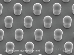
The challenges of this multi-stage wafer testing are compounded by the very dense arrangement of microbumps that form the TSV interconnects between the various layers in the stack. Nearly 4000 microbumps are clustered into tightly packed arrays that form the data paths, power supplies and ground. Most have a diameter of just 25μm and a pitch of 45μm, which demands a high precision probing solution, both mechanically and electrically.
The challenges of this multi-stage wafer testing are compounded by the very dense arrangement of microbumps that form the TSV interconnects between the various layers in the stack. Nearly 4000 microbumps are clustered into tightly packed arrays that form the data paths, power supplies and ground. Most have a diameter of just 25μm and a pitch of 45μm, which demands a high precision probing solution, both mechanically and electrically.

Satisfying mechanical, thermal and electrical parameters, while controlling cost
On the mechanical side, probes must contend with extreme temperatures and test speeds, as well as precision contact with microbumps only 25μm in diameter. On the electrical side, with test speeds of greater than 3Gb/s, impedance control becomes paramount to minimize voltage reflection and crosstalk. To operate at this scale, probes sub-50 μm in diameter (smaller than a human hair) must carry an amp of current, which implies significant heat dissipation, all while avoiding any deformation that would compromise probing accuracy.
FormFactor is thoroughly acquainted with these challenges, which apply not only to HBM, but to a diversity of advanced packaging solutions, such as Intel’s Foveros and TSMC’s Integrated Fanout, as well as others. Through our ongoing collaborations with IC manufacturers and ATE providers, we’ve moved forward with solutions that keep pace with the rapid progress in advanced packaging. For example, we deploy composite metal MEMS probes, sometimes mix-and-match Hybrid MEMS design, in probe cards to deliver finely tuned pitch, high current carrying capacity, and reduced power impedance.
At the same time, we fully realize the need to provide solutions that remain economically feasible in a rapidly changing manufacture/test context. One good example is the role of known good die (KGD) in advanced packaging. It makes sense to test each subcomponent to the point of KGD, but when individual components enter the integration phase, the situation becomes more complex. Take the case of HBM: As each layer of DRAM is added to the stack, to fully test the entire stack each time a new layer is added is a relatively expensive process. The cost of rejection rises as the number of layers increases. At some point, the cost of test outweighs the value added when the system is completed.
At FormFactor, we offer smart test options to achieve the optimal balance between the test cost and test content. For full test coverage KGD test flow, our Altius™ probe card supports 45μm grid-array pitch microbump pitch testing and >3Gb/s at-speed verification. For more mature test flow with acceptable risk for limited test, we also offer the industry’s highest throughput probe card, the SmartMatrix™ product, to dramatically reduce test cost per die. Manufactured by AI-based MEMS probe assembly, SmartMatrix™ allows testing the entire 300mm wafer simultaneously.
Keeping Pace with Technology
While the impact of Moore’s Law on the IC industry may be diminishing, the demand for increasingly powerful micro-circuitry continues unabated. Data centers must prepare for a tsunami of information flow as 5G comes into play. Deep learning via AI will consume CPU cycles at an unprecedented pace. Virtual reality promises to push graphics to ever higher performance thresholds. Autonomous vehicles demand superior real-time performance combined with near perfect reliability.
At FormFactor, we stand ready and able to do our part to ensure that the semiconductor industry keeps pace with this world of accelerating change.