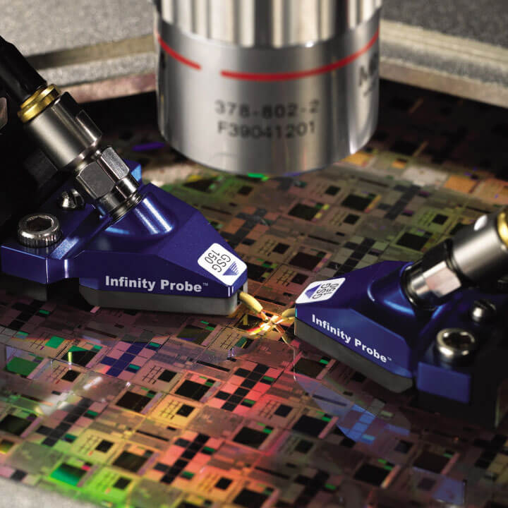
RF on-wafer measurements offer a clear advantage: they allow engineers to assess a device in its raw, unpackaged state. This makes it possible to identify performance issues earlier, before packaging and assembly add cost or potentially introduce additional variables into the measurement.
Accurate device characterization is increasingly important as semiconductor technologies move to higher frequencies and more demanding applications. RF wafer probing provides engineers with a way to understand the intrinsic properties of semiconductor devices and generate the data needed for product development and manufacturing.
In this blog, we’ll cover the fundamentals of RF on-wafer measurements, the types of wafer probers available, the role of RF probes, and best practices for achieving accurate, repeatable results.
Why Are RF On-Wafer Measurements Important?
RF on-wafer measurements allow engineers to characterize semiconductor devices before they are packaged, providing a clearer picture of their RF performance and helping identify problems earlier in the development and manufacturing process.
Testing the device directly on the wafer is important because packaging, interconnects, and assembly can introduce their own electrical effects. On-wafer testing gives engineers access to the device in a less complex environment, making it easier to evaluate performance, compare devices, and identify potential issues before moving further into production.
Types of Wafer Probers
Selecting the right wafer prober depends on the application, test volume, measurement requirements, and desired level of automation. The three primary categories include:
- Manual Probers: Well suited for research environments, educational institutions, and applications where flexibility is more important than throughput. Because positioning is controlled manually, operator experience can play an important role in measurement repeatability.
- Semi-Automatic Probers: These systems add automated positioning and other capabilities that can improve measurement repeatability and accuracy. Features such as automatic thermal drift correction provide a useful balance between operator flexibility and automation.
- Fully Automatic Probers: Equipped with automated wafer handling, these systems are designed for higher-volume environments. They can support continuous testing across wafers and wafer lots with limited operator intervention.
What Are the Key Components of an RF Measurement Setup?
Reliable RF measurements depend on several components working together as a complete measurement system. These typically include:
- RF Probes: RF probes provide the connection between the coaxial or waveguide measurement environment and the planar environment of the device under test. The right RF test probe helps maintain signal integrity while providing consistent contact with the device.
- Power Source and Network Analyzer: A stable power source provides the required device bias, while a vector network analyzer (VNA) measures RF characteristics such as S-parameters.
- Cabling and Calibration Software: Cables connect the VNA to the RF probes, while calibration software helps correct systematic measurement errors and establish an accurate reference plane.
At higher frequencies, the performance of the complete measurement path becomes increasingly important. The probe, cables, instrumentation, calibration, and positioning all contribute to the quality and repeatability of the final measurement.
The Role of RF Probes
RF probes provide the critical signal transition between high-frequency test instrumentation and the contact pads on the semiconductor device. Unlike conventional DC probes, an RF test probe must maintain signal integrity and controlled impedance as signals move between the measurement system and the device under test.
Probe selection depends on several factors, including frequency range, probe pitch, contact pad material, measurement configuration, temperature range, and the characteristics of the device being tested.
FormFactor offers several RF probe technologies designed for different frequency ranges and testing conditions. These include the ACP series, Infinity series, and T-Wave probe series. In addition, the InfinityXF© provides coaxial wafer probing from DC to 250 GHz in a single broadband configuration, supporting high-frequency S-parameter measurements without changing probes across multiple frequency bands.
Selecting the right RF probe is about more than reaching the required frequency. Consistent contact, low loss, repeatability, calibration compatibility, and integration with the overall measurement setup are all important considerations.
Ensuring Calibration and Accuracy
Accurate RF measurements depend on proper calibration. Without calibration, systematic errors such as directivity, transmission tracking, and reflection tracking can affect results and make it more difficult to accurately characterize the device.
Common calibration techniques include:
- SOL (Short-Open-Load) Calibration: Commonly used for one-port measurements, this method corrects system errors using short, open, and load standards.
- SLT (Short-Load-Through) Calibration: Designed for two-port measurement setups and provides correction using short, load, and through standards.
- LRM (Line-Reflect-Match) Calibration: A widely used on-wafer calibration approach that requires fewer assumptions about certain calibration standards and can provide accurate, repeatable measurements.
The right calibration method depends on the device, measurement configuration, frequency range, and accuracy requirements. Calibration should also be considered part of the overall measurement process rather than a one-time setup step, particularly when testing across different temperatures or over extended periods.
Thermal Management and Automation
Temperature changes can introduce measurement challenges by causing physical movement within the test setup. As components heat or cool, probe alignment and contact can shift, potentially affecting measurement accuracy.
Probe systems with thermal management and automation capabilities can compensate for these changes by adjusting probe positioning and helping maintain consistent contact as temperatures change. Automation can also improve repeatability and reduce the amount of operator intervention required during longer or more complex test sequences.
These capabilities become particularly valuable when engineers need to repeat measurements across multiple devices, wafers, frequencies, or temperatures.
For more insights and an in-depth discussion of RF probing techniques, watch our on-demand RF probing webinar.
FAQs – RF Probes and RF Wafer Testing
What is an RF probe?
An RF probe is a specialized test probe used to make electrical contact with RF, microwave, and mmWave semiconductor devices. In wafer testing, the RF probe provides the transition between high-frequency test instrumentation and the planar contact pads on the device while helping maintain signal integrity.
What is an RF test probe used for?
An RF test probe is used to measure the high-frequency electrical characteristics of semiconductor devices. Common applications include S-parameter measurements, device characterization, modeling, RF and microwave development, and mmWave testing.
How is an RF probe different from a DC probe?
A DC probe primarily provides electrical contact for low-frequency or direct-current measurements. An RF probe must also maintain controlled impedance and minimize signal loss, reflections, and other effects that can influence measurements at higher frequencies.
How do you choose the right RF probe?
Choosing an RF probe starts with the required frequency range, but engineers should also consider probe pitch, pad size and material, contact characteristics, measurement configuration, temperature range, and compatibility with the rest of the measurement system.
Why is calibration important for RF wafer probing?
Calibration corrects systematic errors introduced by the measurement system, including the instrumentation, cables, connectors, and probes. This allows engineers to establish an accurate measurement reference plane closer to the device under test.
Can RF probes be used for mmWave testing?
Yes. RF probe technologies can support measurements from traditional RF and microwave frequencies through mmWave and into sub-THz frequencies. The appropriate probe technology depends on the required frequency range and measurement configuration.
Can RF wafer testing be automated?
Yes. Automated and semi-automated probe systems can control wafer positioning, probe alignment, thermal compensation, measurement sequences, and other parts of the test process. Automation can improve repeatability and reduce operator intervention, especially when testing many devices or multiple temperatures.