November 6, 2026
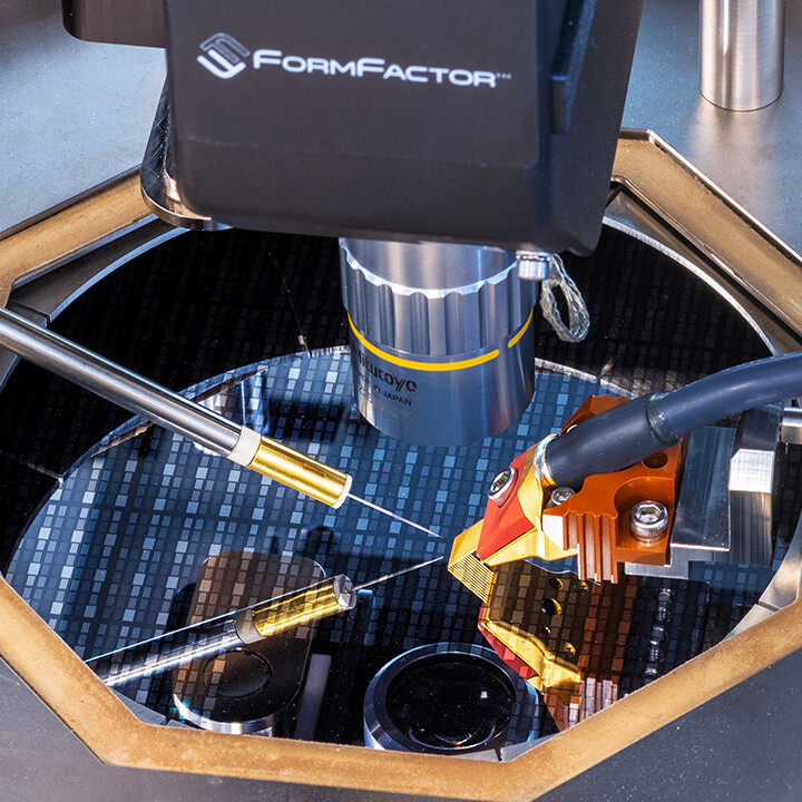
High-voltage probes focus on providing the necessary isolation and safely delivering voltage to the DUT. Dedicated, replaceable probe tips provide contact with the device pad.
November 6, 2026
High-voltage probes focus on providing the necessary isolation and safely delivering voltage to the DUT. Dedicated, replaceable probe tips provide contact with the device pad.
Wide-bandgap semiconductors such as Silicon Carbide (SiC) and Gallium Nitride (GaN) are pushing power devices to higher voltages, temperatures, and power densities. Testing these devices at wafer level brings a new set of electrical, mechanical, and safety challenges.
Applying several kilovolts to a device on an open wafer requires much more than a high-voltage probe with the appropriate voltage rating. The instrument, probe, cables, connectors, chuck, wafer environment, and safety system must work together as one measurement solution.
For engineers developing and testing power semiconductor devices, understanding these interactions is essential for achieving reliable and repeatable wafer-level results.
Wafer-level characterization provides access to important electrical information before devices are packaged.
Measurements such as breakdown voltage, off-state behavior, on-state resistance, and high-current performance can help development teams evaluate device designs and identify process issues earlier. For SiC and GaN power devices in particular, wafer-level characterization can provide valuable insight into off-state and on-state behavior before packaging.
However, high-voltage wafer testing introduces several specific challenges:
Addressing these challenges requires a system-level approach.
Voltage rating is an essential requirement when selecting a high-voltage probe, but it is not sufficient on its own.
High-voltage interfaces are not fully standardized across measurement instruments. Depending on the SMU, curve tracer, or power device analyzer, the system may use coaxial, triaxial, banana, or other high-voltage connections.
The probe and connection package therefore need to match the specific instrument and measurement configuration.
This means considering the complete signal path:
Instrument → Connector → Cable → Feedthrough → Probe → DUT
Every component along this path must be compatible with the instrument and appropriately rated for the intended measurement.
This is also why seemingly simple adapters need careful consideration. Mechanical compatibility between two connectors does not automatically mean that the resulting connection is appropriate for high-voltage operation.
At higher voltages, one of the most significant challenges is electrical discharge.
A major arcing risk occurs at the wafer surface, where pad spacing, exposed structures, passivation openings, contamination, moisture, and neighboring conductive features can produce high local electric fields.
Probe positions are primarily determined by the DUT layout and the location of its pads. Although these pad positions cannot simply be changed to increase probe separation, probe placement, needle condition, and surrounding conductive structures still need to be considered.
The complete high-voltage path must also provide appropriate insulation and electrical clearance.
For some demanding configurations, localized atmospheric control can increase the breakdown strength around the DUT and help suppress corona discharge and surface flashover.
The key is to manage the electrical and environmental conditions where they matter most, particularly around the wafer and probing area.
The importance of system leakage depends on the DUT, operating point, and required current resolution. In some breakdown measurements, DUT current may dominate. For low-current characterization, however, leakage from the probe, cables, chuck, wafer surface, and surrounding environment can remain critical.
Guarding is similarly application- and architecture-dependent. When required, it must be supported by the instrument and maintained through the relevant measurement path.
The measurement architecture should therefore follow both the capabilities of the selected instrument and the requirements of the device measurement.
Power device characterization often combines two very different measurement requirements.
In the off-state, the DUT may be exposed to several kilovolts at relatively low current. In the on-state, the measurement may require significantly higher current at much lower voltage.
These operating conditions place different requirements on probes and signal paths.
High-voltage probes focus on providing the necessary isolation and safely delivering voltage to the DUT. Dedicated, replaceable probe tips provide contact with the device pad.
High-current probes, on the other hand, are designed to minimize contact resistance and distribute current effectively. Multi-finger probes can distribute current across the pad, reducing localized current density and contact resistance.
The chuck is equally important. For vertical power devices in particular, it can provide the backside electrical connection and therefore become part of the measurement circuit. A low-resistance chuck path and Kelvin sensing can help reduce the influence of connection resistance on high-current measurements.
Power semiconductor testing may involve thin, warped, or TAIKO wafers that require controlled handling and vacuum support.
An unsuitable vacuum configuration can deform a thin wafer, affect backside contact, or potentially damage the substrate.
A chuck designed for thin-wafer testing can use controlled vacuum zones to provide stable support. Controlled wafer support helps maintain repeatable positioning and backside contact during measurement.
This makes wafer handling an important part of the overall measurement environment, rather than simply a mechanical consideration.
High-voltage wafer testing involves exposed wafers, movable probes, and potentially hazardous voltages. Safety therefore has to be designed into the system from the beginning.
A high-voltage safety concept can include:
The safety interlock has to be coordinated with the measurement instrument, so hazardous voltage cannot remain active when the protected area is accessed.
This integrated approach helps protect both the operator and test equipment while supporting efficient wafer-level operation.
Reliable high-voltage wafer testing requires a system-level approach, from the measurement instrument and probe to the chuck, wafer environment, and safety architecture.
The right solution starts with the measurement instrument and DUT, then considers the probe, connection path, chuck, wafer handling, arcing control, high-current requirements, and safety architecture.
FormFactor brings these elements together in integrated wafer-test solutions that can include:
Engineering these components as part of a complete measurement environment turns high-voltage capability into more than a specification of an individual probe.
It creates a reliable, application-specific measurement path from the instrument to the DUT.
Start with the measurement instrument and required voltage capability. Because high-voltage interfaces are not fully standardized across instruments, the probe, cable, connector, and connection package should match the specific SMU, curve tracer, or power device analyzer as well as the application requirements.
No. Voltage rating is essential, but it is only one part of the measurement system. Instrument compatibility, cables and connectors, chuck configuration, DUT layout, environmental conditions, and the safety concept all influence the usable high-voltage capability.
A major arcing risk occurs at the wafer surface, where pad spacing, exposed structures, passivation openings, contamination, and environmental conditions can create high local electric fields. Appropriate insulation and clearance are also required throughout the complete high-voltage path.
No. Guarding depends on the measurement instrument, measurement architecture, and application. When guarding is required, it needs to be supported and maintained through the relevant measurement path.
Typically, different probe designs are used because the measurement requirements differ. High-voltage probes focus primarily on isolation and safely delivering the required voltage, while high-current probes are designed to minimize resistance and distribute current effectively. An integrated wafer-test solution can support both requirements with the appropriate probes, chuck, connections, and instrumentation.
As power semiconductor technologies continue to evolve, wafer-level testing must keep pace with increasing voltage, current, thermal, and safety requirements.
Successful high-voltage wafer testing starts by looking beyond the probe itself. Understanding the instrument interface, electrical path, DUT and wafer conditions, chuck configuration, and safety architecture helps create a test environment designed for reliable and repeatable measurement results.
Planning a high-voltage wafer-test application? Talk to FormFactor about an instrument-specific probing and measurement solution for your device, wafer, and test requirements.