Stay Connected
Receive product updates and event notifications
Subscribe to Our NewsletterFormFactor is a leading provider of essential test and measurement technologies along the full IC life cycle – from characterization, modeling, reliability, and design de-bug, to qualification and production test.
Receive product updates and event notifications
Subscribe to Our NewsletterCascade 300 mm probe stations set the standard for manual and automated on-wafer test, delivering the precision and versatility needed to address a wide range of advanced, complex testing requirements.
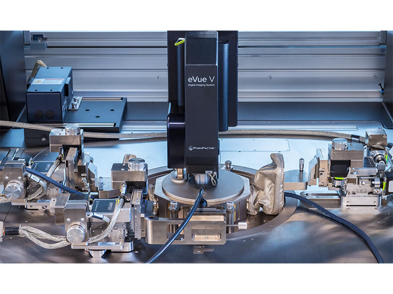
FormFactor’s Contact Intelligence technology combines smart hardware design and innovative software algorithms to provide accurate probe-to-pad alignment and electronic recalibrations in engineering labs and many production applications. FormFactor now has specialized Contact Intelligence assistants for autonomous RF, DC and Silicon Photonics (SiPh) testing.
The broad use of power semiconductors has created a pressing need to characterize power devices quickly and efficiently. FormFactor offers on-wafer power device characterization systems to reduce time-to-market for new power devices and to keep up with production.
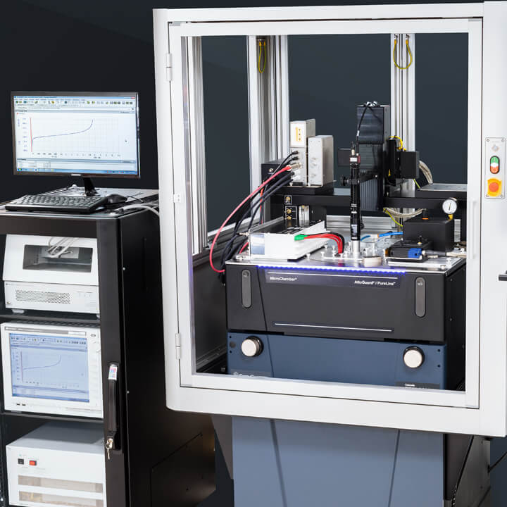
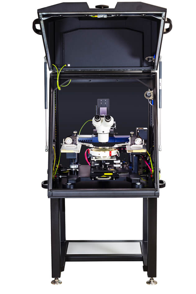
Autonomous High-Power wafer probing featuring Contact Intelligence
300 mm semi-/ fully-automated on-wafer power device characterization system
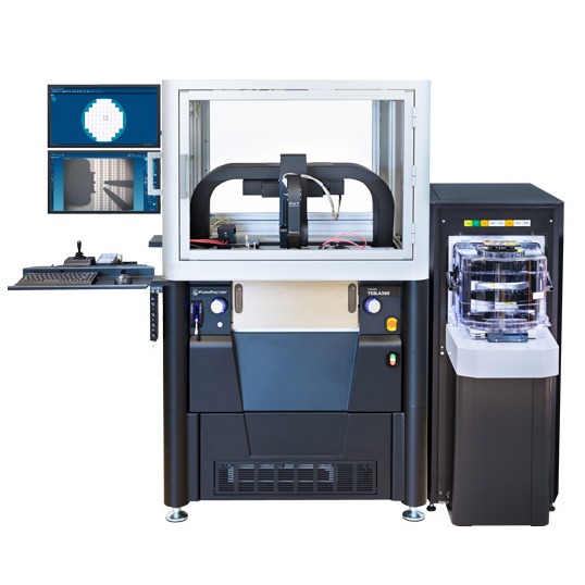
200 mm semi-/ fully-automated on-wafer power device characterization system
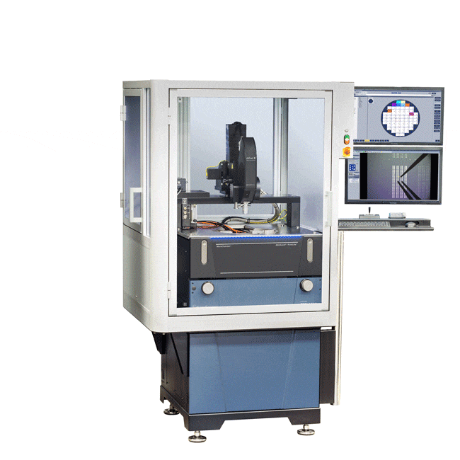
150 mm manual on-wafer power device characterization system
FormFactor’s IMS products deliver robust, turn-key functionality, peace of mind, and a faster path to collecting high-quality on-wafer measurement data for today’s important and challenging test applications. Integrated Measurement Systems unite instruments and other products from FormFactor’s partners, including Keysight Technologies, along with FormFactor’s probe systems, probes, and everything else needed to deliver critical data for devices and integrated circuits on the wafer.
Receive product updates and event notifications
Subscribe to Our Newsletter