Contact Us
Connect to an Expert

Looking for customer support? Ready to learn more about our products and services?

Contact Sales Today
  • TESLA200 High Power 200 mm Probe System
  • TESLA200 Fully-Automated High Power Probing System
  • TESLA200 Fully-Automated High Power Probing System
  • On-wafer Power Device Characterization System

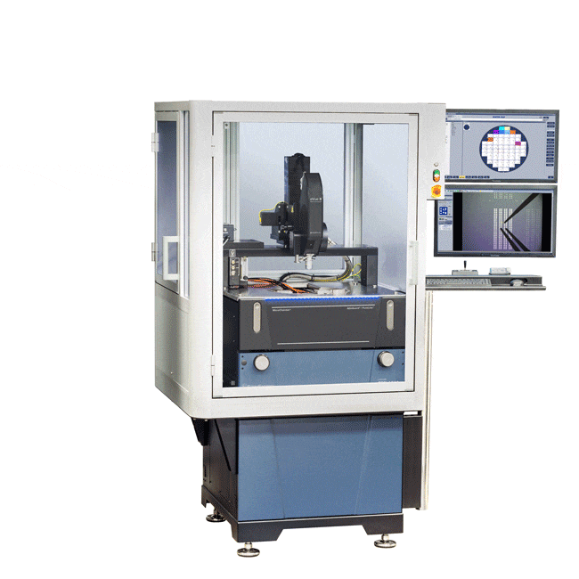
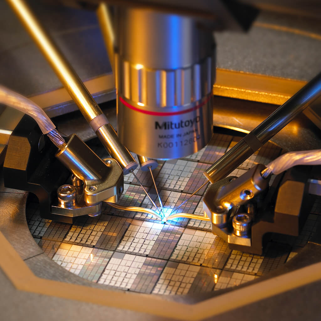
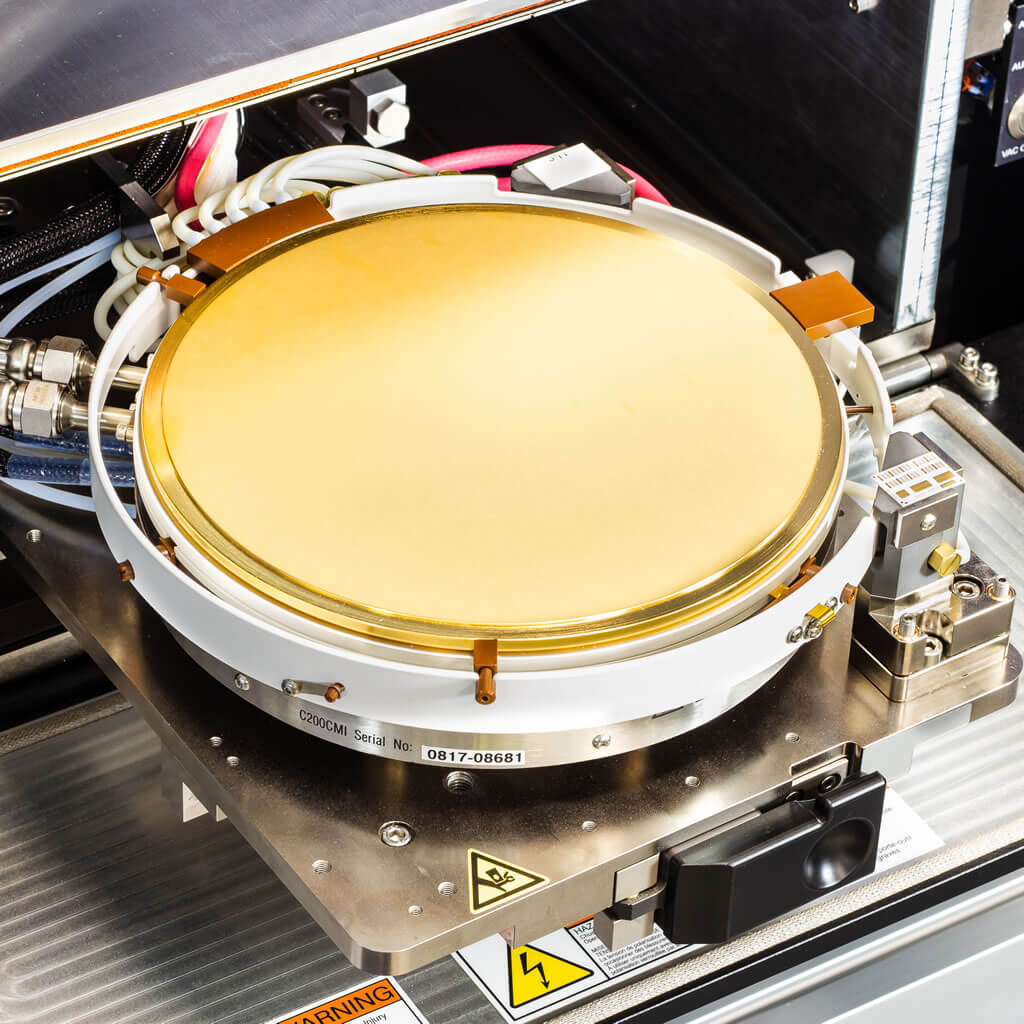
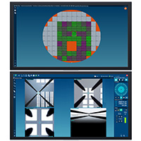
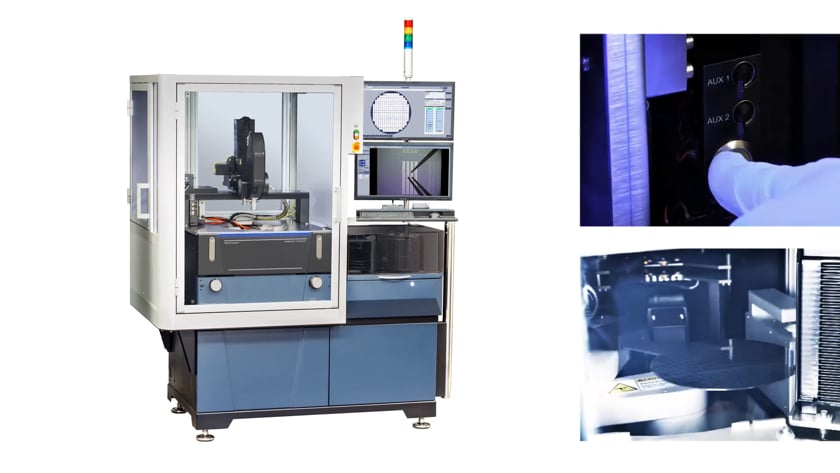
Designed specifically for IGBT/power MOSFET (GaN, SiC, Si) device measurements at the wafer level, the new TESLA200 on-wafer power semiconductor probing system is engineered to provide accurate data up to 3 kV (triaxial) / 10 kV (coaxial) and 200 A (standard) / 600 A (high current). With next generation test capabilities, anti-arcing solutions, wafer automation, and support for both engineering probes and T.I.P.S. “LuPo” High Voltage / High Power Probe Cards, the TESLA200 now enables complete thermal testing (-55°C to 300 °C) with fully-automatic thinned/warped/TAIKO wafer loading. One system covers all on-wafer high power test needs, from R&D to niche production.

The new TESLA200, available in semi-automatic and fully-automatic models, is scalable and field upgradeable, allowing it to meet any budget requirements. The system is ideal for collecting high accuracy measurement data on single or volume wafers as fast as possible, and can be utilized in R&D, device characterization/modelling or niche production applications.

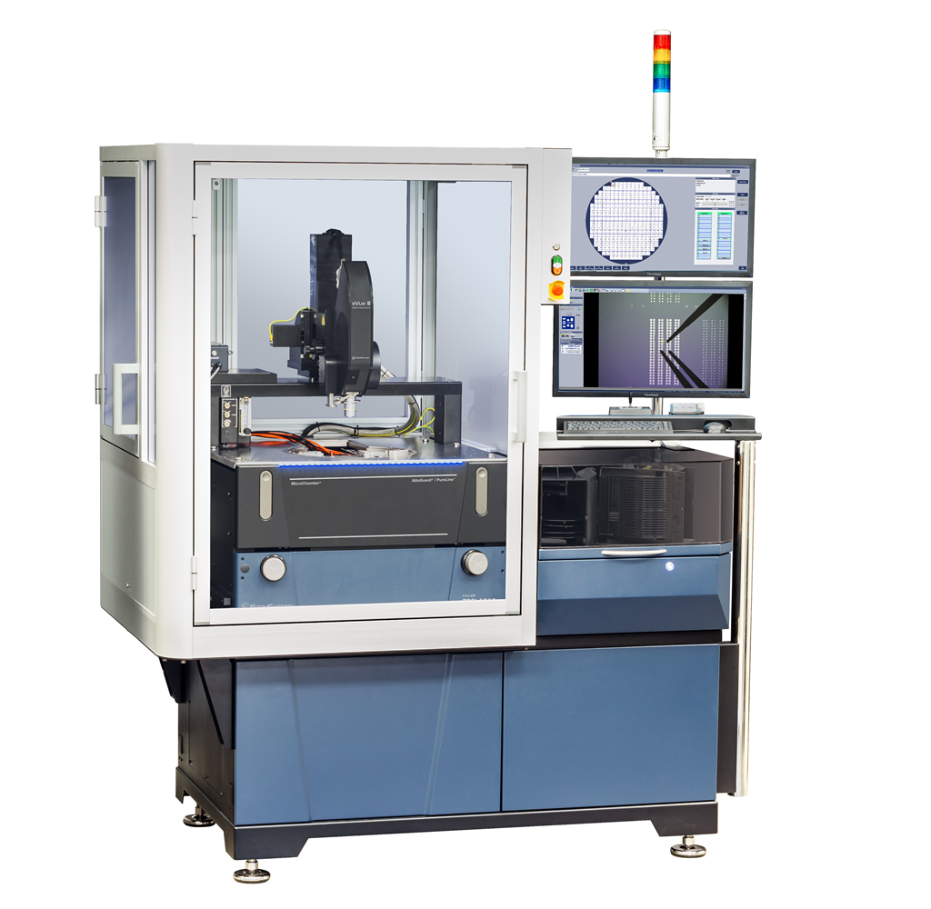
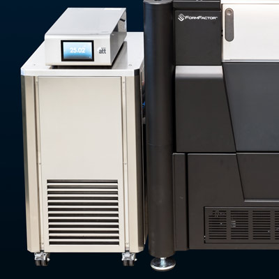
Patented AttoGuard® and MicroChamber® technologies built in TESLA200 significantly improve low-leakage and low-capacitance measurements. In combination with FormFactor’s patented TESLA FemtoGuard™ thermal chuck technology, the TESLA200 provides an ultra-low noise, fully guarded and shielded test environment. The high-power TESLA FemtoGuard chuck also incorporates MicroVac™ technology enabling low-contact resistance, thin-wafer handling and maximum power dissipation.

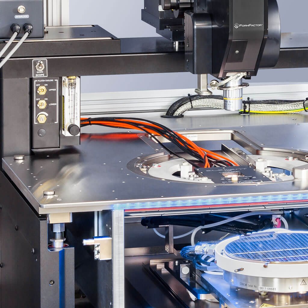
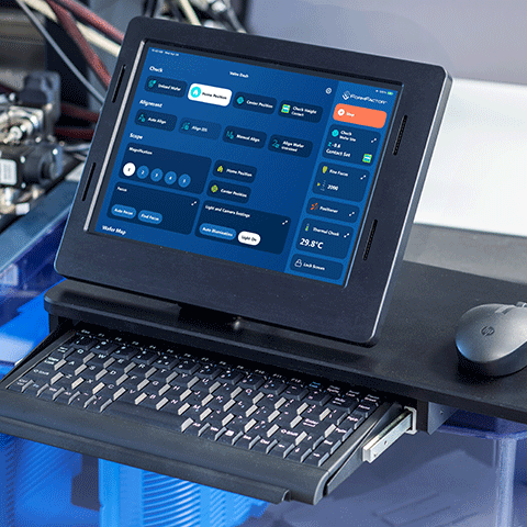
To ensure the utmost safety during high-voltage measurements, the TESLA200 on-wafer power semiconductor probing system employs a TUV-certified safety interlock system integrated with an ergonomic clear enclosure. With an advanced 200 mm fast stage, automatic wafer loader and thin wafer handling capability, TESLA200 provides everything needed for scientists, R&D / test engineers, or production operators to get their job done fast.

High-voltage/current Probes

High-voltage/current Probes

  • On-wafer power device characterization up to 10,000 V DC / 600 A
  • Reduced probe and device destruction at high currents up to 20 A DC and 300 A pulse
  • Increased isolation resistance and dielectric strength to provide full triaxial capability at high voltage (3,000 V) for low-leakage measurement

TESLA200 High Power Probe Station with High-voltage Anti-Arcing Probe Card from T.I.P.S.

T.I.P.S. “LuPo” High Voltage / High Power Probe Cards

Gold-plated TESLA High-power MicroVac Chucks

Gold-plated TESLA High-power MicroVac™ Chucks

  • Prevent thin wafers from curling and breaking
  • Advanced MicroVac chuck surface for minimum contact resistance between wafer and chuck
  • Accurate Rds(on) measurement at high current
  • Accurate UIS measurements at high temperature

On-wafer Power Device Characterization System

Safety for Operator

  • Safety interlock system with clear enclosure for operator safety during device measurements
  • Roll-out stage for full wafer access and easy wafer loading/unloading

Safe High Power Probe System Integration

Seamless Integration

  • Convenient connection kits for easy and safe system integration with power device analyzers from Keysight Technologies and major suppliers
  • Seamless integration between Velox and analyzers/measurement software

Probe Station with Economic Thermal System

Thermal Measurements

  • Wide range of extremly performant, reliable thermal chuck systems from ATT
  • Flexibility from hot only to full thermal range of -60°C to +300°C
  • Up to 25% lower air consumption (CDA) than other systems in the market (300l/min) with no compromise in transition times
  • Up to 15% faster transition times than other systems in the market
  • Patented MicroVac™ and FemtoGuard™ Technologies, providing ultra-low noise measurements and controlled leakage, low residual capacitance for repeatability and advanced measurement accuracy and speed
  • Field-upgradeable: grows with your needs

Velox Probe Station Control Software

Velox Probe Station Control Software

  • User-centered design minimizes training costs and enhances efficiency
  • Windows 10 compatibility enables highest performance and safe operation with state-of-the-art hardware
  • Comprehensive alignment functions – from simple wafer alignment and mapping to advanced probe-to-pad alignment over multiple temperatures for autonomous semiconductor test
  • Simplified operation for inexperienced users: Reduced training costs with Workflow Guide and condensed graphical user interface
  • Loader integration – Easy creation of workflows and receipts and no need for any additional software
  • VeloxPro option: SEMI E95-compliant test executive software that enables simplified and safe automation of the entire wafer test cycle

  • High Power

vimeo-video-thumbnail

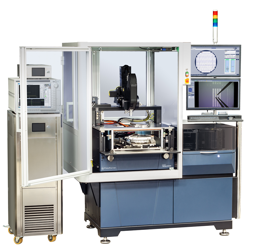
TESLA200 - 200mm High Power Probe System

The TESLA200 Advanced On-Wafer Power Semiconductor Probe System is an integrated high-power test solution that enables collection of accurate high voltage and high current measurement data, with complete operator safety.
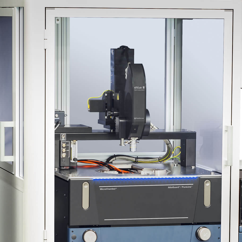
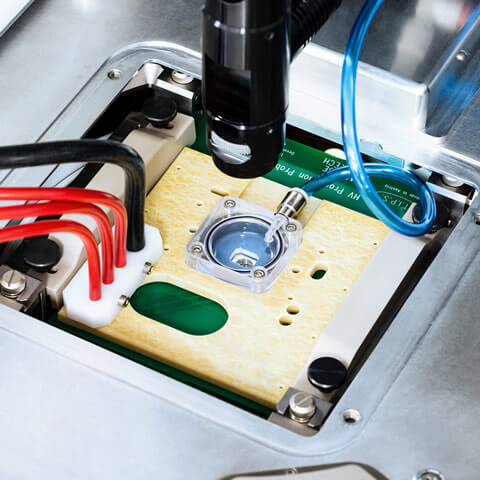

vimeo-video-thumbnail

eVue IV Microscope

The eVue IV digital imaging system combines extraordinary optical performance with increased productivity.


vimeo-video-thumbnail

SourceOne – Certified Pre-Owned Equipment

You want the best price-performance ratio for your wafer probe station? With our Certified Used Equipment we have an attractive option for you.

vimeo-video-thumbnail

SourceOne – Factory Refurbishment Program

Extend the use of your probe station for up to another 15 years with our Factory Refurbishment Program.

vimeo-video-thumbnail

SourceOne – Trade In / Buy Back Program

We'll take your probe station back for a credit note.