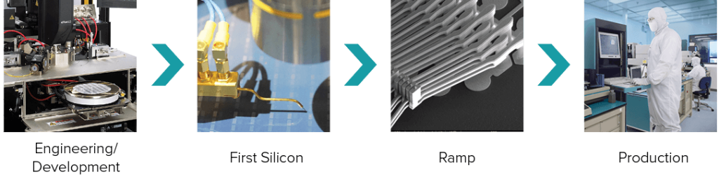
Test Expertise—
from Lab to Fab
When market pressures demand the shortest possible path from concept to volume production.
The pressure to bring products to market with no flaws, at the lowest cost, and at an accelerated pace puts focus directly on how products are tested throughout the flow of development through manufacturing.
As semiconductors move from the test lab to manufacturing, massive amounts of data must be extracted and analyzed to ensure ultimate success in the marketplace. It’s a process that starts before the first wafer is fabricated and continues all the way through final packaging. Each phase produces information vital to successive phases. What’s learned in the lab moves forward and becomes critical to efficiency on the production floor.
Adding Value Along the Design to Test Continuum
FormFactor is in the unique position to add value along all the steps of the process of semiconductor validation and test. The company offers a full spectrum of proven probe technologies for every phase, as well an unmatched depth of expertise in how to best integrate it into the overall test and measurement process. Through intense collaboration with both customers and partners, we continually produce solutions that minimize the time and cost of test, while maximizing accuracy and efficiency. And since test consumes a large portion of a fab’s capital budget, a very tangible contribution toward increased profitability can be attained.
How a Lab to Fab Test Perspective Helps Advanced Technologies
Two relatively new IC technologies, high-bandwidth memory (HBM) and silicon photonics, illustrate how we participate in moving an emerging technology from lab to fab with maximum efficiency. HBM stacks multiple layers of DRAM die atop each other and uses fine-pitch silicon interposers to interconnect them with a GPU or CPU subsystem. This tight physical proximity on a single substrate maximizes both performance and integration. However, it also creates some advanced testing challenges. Working with HBM design engineers at the conceptual stage, we are able to anticipate the complex technical and economical requirements posed by production test.
The ultimate solution can involve a combination of products to achieve optimal yield while achieving the lowest cost of test. In this case, the solution involved three elements: one type of probe card for massive parallel testing of the DRAM on sacrificial test access pads between microbumps, and a second type for testing the singulated die or stack with grid arrays of microbumps of 25 µm diameter for full functional test, and a third type to test the quality of silicon interposers to ensure TSV connectivity for critical I/Os. We help our customers when they are ready for testing and their HBM products are ready to enter the market in volume.
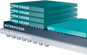
Sample architecture of an advanced package stack
When Test and Validation Methodologies Haven't Been Established Yet
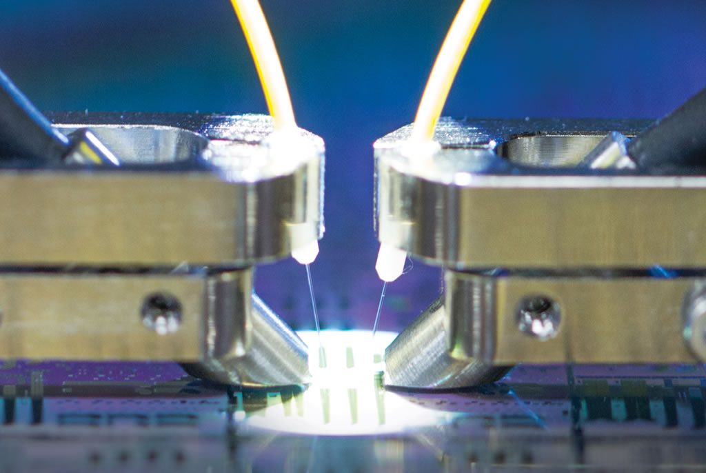
Silicon photonics (SiPh) is an example of a technology that is both in the lab and entering the early stages of production. By fabricating optical devices in CMOS, SiPh can enable the economies of scale needed for data centers to meet ever increasing bandwidth demands while reducing power consumption and heat dissipation. Additional promising technologies for SiPh include biological sensing, LIDAR remote sensing, quantum computing. The technology is new enough that the industry has yet to settle on an established set of test and validation methodologies. To reach this point, we are actively developing technology and techniques along with key suppliers in the instrument and positioning fields to create a standardized path from initial validation though volume manufacturing.
Applying Our Expertise Towards Practical and Profitable Customer Applications
With over 25 years of industry leadership, FormFactor has accumulated a massive knowledge base of probe technology and products, with expertise in how to best integrate them into test systems encountered around the globe. In fact, this experience extends all the way back to fundamental research and development—even before new chip technologies are productized or standardized. Our mission is to help translate this advanced knowledge into practical and profitable applications as emerging technologies find their way into products in common use around the world: a wireless transceiver in a cell phone, a collision-avoidance radar system in an automobile, or a GPU for virtual reality in a gaming system.
For both emerging and established semiconductor technologies, our unmatched expertise in wafer probing and measurement is continually enriched through our collaboration with our partners in the instrumentation and production test fields. It produces a spirit of exploration and discovery that energizes all of our engineering efforts, from initial device characterization in the lab through high-volume production test in the fab.
Insights Enhance Yield Knowledge, Cost Efficiencies and Acceleration to Profitability
FormFactor combines its strength in engineering development and manufacturing in a unique “Lab to Fab” semiconductor test and measurement solution set. With a collaborative style, a deep knowledge base, and a global footprint that enhances accessibility to experts, the company addresses today’s most advanced technologies and takes aim at lowering costs and accelerating time to profitability for its customers.
If you are faced with the ever-increasing pace of change and trying to achieve the perfect balance of quality, cost and time to market, you can turn to the one company with insights and experience in semiconductor test and measurement solutions from the lab to the fab—FormFactor. The company with over 25 years of delivering unmatched test and measurement expertise at every stage of the design to production test continuum.