Cascade
|Z| Probe® PCB
Robust RF test on PCB and ceramic
Robust RF test on PCB and ceramic
Looking for customer support? Ready to learn more about our products and services?
Contact Sales TodayReceive product updates and event notifications
Subscribe to Our Newsletter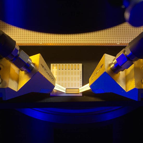
Flexibility is the key for efficient PCB and ceramic testing. The |Z| Probe® PCB is simple to align and handle and can be easily positioned. It optimally replaces costly test fixtures which are often inflexible. A robust design makes the |Z| Probe PCB easy to handle and offers a long working life typically more than one million (1,000,000) contacts.
The planar tip of the |Z| Probe PCB has precisely calculated, parallel, separate contact springs which move independently of one another, allowing a precise, quick and simple contact with the DUT, even if there are significant contact height differences. This unique feature as well as the overall very robust design of the |Z| Probe PCB ensures a long life and simple handling.
Used in conjunction with a manual probe system including probe positioners and calibration substrates, the |Z| Probe PCB becomes the ultimate tool for all RF circuit probing needs.
Receive product updates and event notifications
Subscribe to Our Newsletter