Wafer-Level Testing for AI Processors
Artificial Intelligence (AI), once confined to science fiction, now impacts daily life. From voice assistants and autonomous vehicles to healthcare diagnostics and supply chain optimization, AI is reshaping industries.
At the core of AI lies its neural network architecture, which mimics the way biological brains process information—recognizing patterns through repetition and example, as opposed to the sequential logic of traditional programming. These neural networks consist of vast arrays of interconnected nodes, each functioning like a synthetic neuron. Each node acts as an independent algorithm, exchanging data to collectively solve complex problems. To train and refine these models, immense computational power is needed to simulate the behavior of each node through countless cycles. This demand for high-performance processing makes AI an ideal candidate for cutting-edge semiconductor technologies capable of massive parallel computation.
As AI evolves, specialized hardware and testing solutions to support these parallel workloads are increasingly critical. The rapid expansion of AI applications—from autonomous driving and edge computing to high-performance computing (HPC) and 5G networks—has placed unprecedented pressure on semiconductor manufacturers to deliver chips that can perform at scale while maintaining energy efficiency and reliability.
Making Wafer-Level Probe Solutions for Artificial Intelligence Possible
AI’s computational power relies on innovative semiconductor technologies and specialized testing solutions. To meet the demands of AI chips, wafer-level probe solutions must offer precision, scalability, and reliability during testing. With billions of transistors and complex packaging, including 2.5D and 3D stacking, probing these advanced chips efficiently and accurately presents a significant challenge. As AI drives new innovations, understanding how semiconductor technologies enable these advancements is critical. The rise of large language models (LLMs) and other AI applications is fueling the need for cutting-edge semiconductor solutions, such as advanced packaging, hybrid MEMS technology, and precision testing. These technologies are essential for achieving the performance and efficiency required by modern AI processors.
Advanced AI Requires Advanced IC Packaging
What once required the raw power of supercomputers is now achievable through advances in integrated circuit (IC) technology. Today’s AI chips feature billions of transistors packed onto a single substrate, providing unprecedented processing power in compact form factors.
A key innovation enabling AI’s computational strength is advanced packaging, which positions multiple logic functions in close proximity to optimize both speed and energy efficiency—crucial for high-performance AI applications. In this new era of AI hardware, heterogeneous integration—where memory, logic, and sensors are combined into a single package—has become a major trend. This integration allows for faster processing but also introduces challenges related to packaging complexity, interconnect density, and testing. Advanced techniques like 2.5D and 3D stacking are now widespread, particularly in AI accelerators and high-performance processors, driving the need for highly specialized probing solutions.
VIDEO: Solving the challenges of very high power and very high signal count with hybrid MEMS technology.
AI Processor Architecture
AI processors are designed to handle the high-throughput, parallel processing tasks essential for training and running neural networks. These processors typically feature multi-core architectures, specialized accelerators (e.g., GPUs or TPUs), and high-bandwidth memory to maximize computational efficiency. The dense packaging of these processors adds complexity to their testing, requiring precise wafer-level probing techniques to ensure they meet performance and reliability standards.
AI Chip Testing
Testing AI chips requires specialized wafer-level probing solutions that accommodate high-density interconnects and fine-pitch microbumps. These tests ensure that chips can manage the massive parallel workloads of AI applications, from machine learning to autonomous vehicles. FormFactor’s probe cards are engineered for precise, repeatable testing of high-performance AI chips, ensuring scalability and reliability throughout production.
Microbump Probing
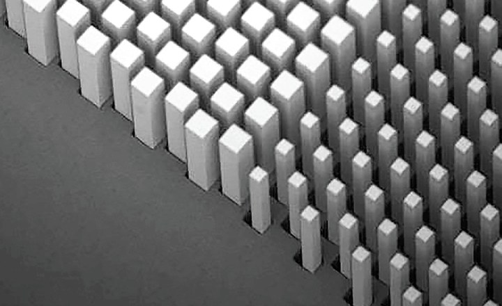
AI chips often rely on microbumps—tiny test points that connect data paths, power supplies, and ground connections—to enable high-density packaging. Probing these microbumps is essential for verifying chip performance. With bumps as small as 25 μm in diameter and placed as close as 45 μm apart, testing requires extreme precision. FormFactor’s advanced probing solutions are designed to handle these tight tolerances, ensuring reliable results for high-performance AI processors.
Probing the Inner Limits
AI-driven chip designs, particularly those using advanced packaging, present unique testing challenges. Each layer of these sophisticated chips must be tested before being stacked into the final die. Testing often involves probing up to 4,000 microbumps—tiny test points connecting data paths, power supplies, and ground connections. These microbumps can be as small as 25 μm in diameter and placed just 45 μm apart, making them a fine target for testing.
The challenge is further complicated by heat generation. High-density chips can produce significant heat during probing, potentially damaging the probes or skewing test results. As AI workloads demand continuous, massive parallel processing, maintaining precise thermal control during testing is essential to preserving the integrity of both the test and the device.
At FormFactor, we’ve developed next-generation wafer probe cards capable of landing on microbumps as small as 25 μm in diameter—smaller than a human hair. Our proprietary MEMS technology and specially formulated metal alloys allow each probe to carry over an amp of current without overheating, ensuring precise testing during extended, high-performance test cycles and preventing damage to both the probe and the device.
Hybrid MEMS probing technology for high bandwidth memory
Hybrid MEMS Insights: FormFactor’s CTO Jarek Kister explains how FormFactor’s Hybrid MEMS technology enables engineers to balance contact force, high current carrying capability, and ultra-fine pitch to optimize advanced wafer probe requirements.
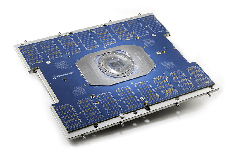
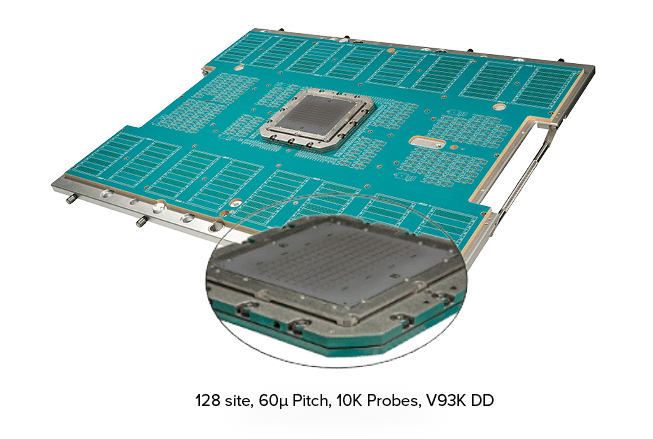
Apollo Probe Card
| FormFactor’s Apollo™ vertical probe cards are designed for high-density applications like area-array and perimeter-layout probing. These cards are the leading solution for testing high-performance chips such as graphics processors, game console microprocessors, and automotive microcontrollers. Apollo™ offers superior reliability, scalability, and production efficiency, making it the preferred choice for multi-DUT (Device Under Test) testing in high-volume manufacturing.
|
 |
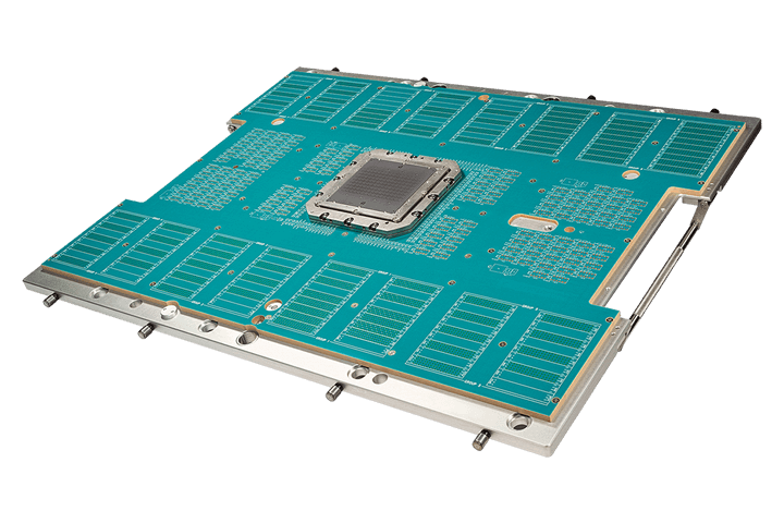
Kepler ™ Probe Card
FormFactor’s Kepler™ vertical probe cards address the challenges of testing large active areas, particularly in applications like automotive electronics, IoT devices, and industrial uses. Kepler™ cards feature thermally stable vertical springs that accommodate wide temperature ranges, a critical factor for high-performance, high-reliability testing in demanding environments.
- Multi-layer ceramic (MLC) space transformer for efficient signal routing
- Proprietary fine-pitch, low-force 2D MEMS springs for precise, minimal-contact probing
- Full planarity and tilt adjustment for accurate contact across various devices
- Multi-site testing (X8–X16) with ultra-high pin counts (20–30k pins)
- Flexible probe head configurations supporting diverse device layouts and pad pitch requirements
- Field-replaceable springs and components for easy maintenance
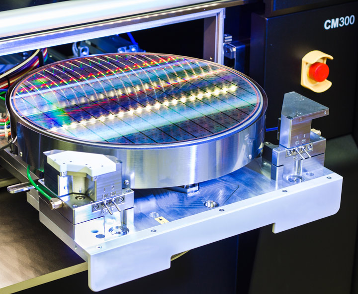
Active Thermal Control: Managing Heat for Reliable Testing
We also provide solutions that continually control the temperature of the chuck, which holds the wafer in place during probing. Temperature sensors constantly monitor the interface between the chuck and wafer, with liquid cooling applied to keep heat levels within acceptable limits.
In addition to precision probing, managing temperature during testing is critical. To mitigate the risk of overheating and ensure accurate results, FormFactor offers active thermal control systems to regulate the temperature of the chuck (the platform holding the wafer). Temperature sensors monitor the interface between the chuck and wafer, while liquid cooling systems maintain heat within acceptable limits. This thermal management is especially important for AI chips, which generate significant heat during prolonged, high-performance testing.
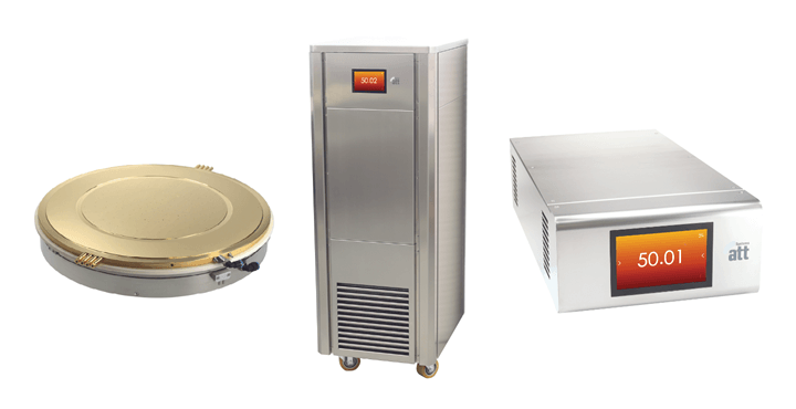
Active temperature control is essential – the Thermal Chuck plays a key role in maintaining optimal conditions within the test cell.
Supporting the Future of AI with Advanced Wafer Probe Solutions
As AI continues to revolutionize industries—from autonomous driving and edge computing to cloud services and high-performance computing (HPC)—FormFactor is committed to delivering cutting-edge wafer probe solutions that meet the evolving needs of this transformative technology. Our advanced probe technologies, including Hybrid MEMS, Apollo™, and Kepler™ probe cards, ensure precise, scalable, and reliable testing for the next generation of AI chips.
Through ongoing innovation, FormFactor remains at the forefront of driving AI advancements and semiconductor breakthroughs.