Contact Intelligence—
When Precise Contact Matters
Innovative probe system technology senses and reacts to enable autonomous semiconductor test.
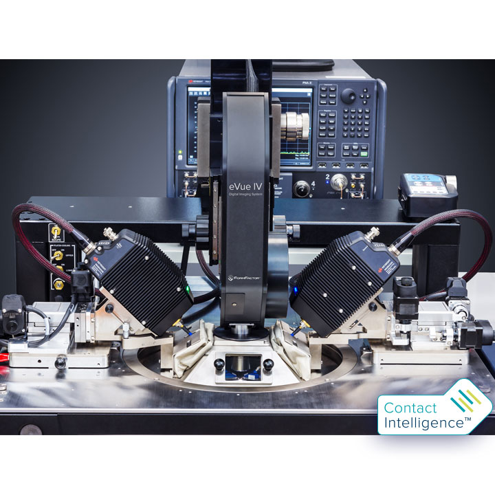
FormFactor has developed an integrated suite of tools for the engineering lab to optimize probe contact accuracy on wafers to deliver precise measurements enabling true, autonomous test. From sensitive temperature testing environments in RF or DC applications, all the way to silicon photonics where precise placement of light in test situations is critical, Contact Intelligence accelerates time to accurate data, in some cases, reducing test time from months to minutes.
FormFactor’s Contact Intelligence combines smart hardware design, innovative software algorithms and years of experience to create a technology that provides benefits across a wide array of applications in device testing.
Wafer-Level Test Faces Mounting Pressure
Global technology trends, such as the move to 5G, are creating a growing demand for new generations of ICs that are faster, more energy efficient, and able to operate in environments all the way from outer space to the engine compartments in self-driving vehicles.
Given this relentless advance in technology, wafer-level test has become increasingly complex and time-consuming in response. Large volumes of data must be extracted under diverse conditions to guarantee performance, validate fab processes, and measure life cycles, among other requirements.
At the same time, market pressures make no allowance for extra time to be spent, either in the lab or the fab, on wafer-level testing. Engineers and scientists need to find ways to leverage scarce human resources to keep pace.

Contact Intelligence Accelerates Time to Accurate Data, Time to Market and Ultimately—Time to Profitability

The solution has come in the form of new technology, innovative hardware and software that accelerates the testing cycle in the engineering lab—with no loss in measurement accuracy. And since wafer probing is a key part of IC test and measurement, it presents a major opportunity to streamline the overall process.
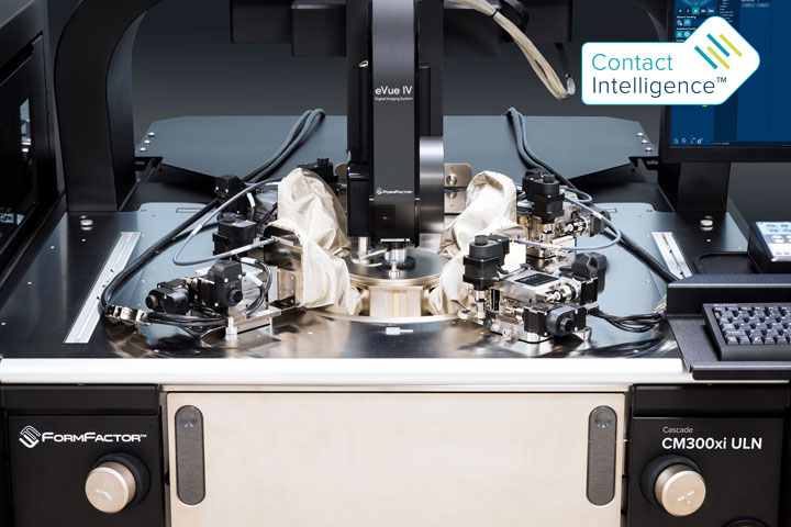
In the lab or in niche-production, we refer to this new breed of technology as Contact Intelligence, and it’s already found its way into our more advanced wafer probe stations. The following are a few instances of how Contact Intelligence is being applied.
Compensating for Thermal Drift
Many wafer probing scenarios now involve characterizing device behavior over an ever-wider range of temperatures. Ranges of -40°C to 125°C are not uncommon, with wafer reliability testing up 300°C. Typically, tests are conducted at up to four set points, and due to linear expansion, each requires a significant realignment of probe tips to accurately contact pads on the device under test. Two phenomena come into play here, one involving the times required to stabilize the probe system at a new temperature, and the other involving the position of the thermally controlled chuck/wafer in relation to the platen. Both affect the probe-to-pad alignment.
As the chuck temperature rises, it heats the platen above it. Once the assigned chuck temperature is reached, there is a delay before the system as a whole comes into equilibrium. The amount of delay is variable and depends on the temperatures involved. Contact Intelligence allows the system to sense these preset temperatures and then respond by waiting the correct amount of time until the system is stabilized. This allows lengthy test routines to be conducted without operator intervention.
Dynamic Probe to Pad Alignment
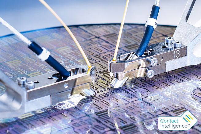
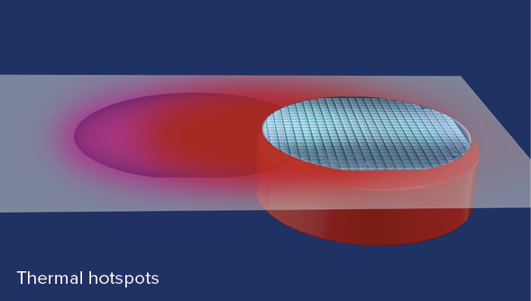
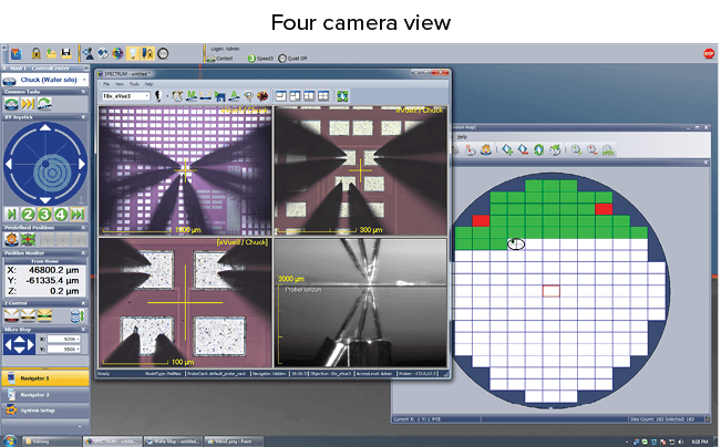
Even after thermal equilibrium is reached at the system level, a second adjustment is often required due to “hot spots”, which occur when the chuck moves to test a new die at a new location on the wafer. Contact Intelligence senses these changes and reacts when the new test location has stabilized. Once this stabilization has occurred, Contact Intelligence’s on-site Probe-to-Pad Alignment (PTPA) correction technology uses advanced image processing algorithms and precision positioning to perform the final probe-to-pad alignment.
Although the on-the-fly alignment of the overall probe-to-die location is correct, in many cases the probes themselves will have expanded or contracted with temperature, which means the probes will have excessive or insufficient over-travel.
With large pads, this is not a significant problem, but as devices move to smaller pads, this represents a real challenge. In this case, probes tend to skate off the small pads or do not make adequate contact for a good electrical connection.
To overcome this problem, Contact Intelligence’s combination of smart software, probe tip recognition algorithms and advanced programmable positioners can automatically compensate to optimize probe positioning contact to each pad being probed. This is done on-the-fly to ensure each die tested is as good as the last. And, of course, this is needed for both DC and RF probing applications.
Contact Intelligence for RF Device Modeling
With the demand for faster time to market for new high frequency IC’s in markets such as 5G, self-driving vehicles and next generation Wi-Fi, IC designers need the highest quality process design kits (PDK’s) from the foundry or fab in order to make sure their designs work on the first iteration. Poor PDK’s will lead to more design iterations and not meeting product launch time expectations. In order to make more accurate PDK’s, foundries and fabs need to ensure they make the highest precision measurements and measure more test structures to improve device models that make up the PDK’s.
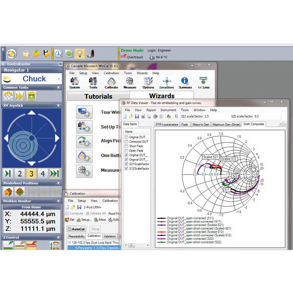
Normal testing of RF device modeling test structures requires large amounts of time from the engineer to perform re-calibrations whenever the system drifts beyond a usable limit, which is unavoidable with Vector Network Analyzers. Re-positioning of the probes when changing temperature, also requires user intervention. With FormFactor’s Contact Intelligence, the operator can start a test and leave the system measuring during the whole shift, overnight or even over the weekend, without any user intervention. Contact Intelligence offers true hands-free and autonomous RF calibrations and measurements over multiple temperatures. Programmable positioners and, probe tip recognition algorithms coordinate with our WinCal XE calibration software to automatically recalibrate if the system performance drifts beyond a usable limit. Probes are dynamically corrected for the most accurate pad placement on-the-fly to compensate for any thermal expansion of the probes or device when changing temperature. This results in testing more devices in a shorter period of time, with a higher degree of confidence in the RF measurement performance, leading to more accurate PDK’s and faster time to market.
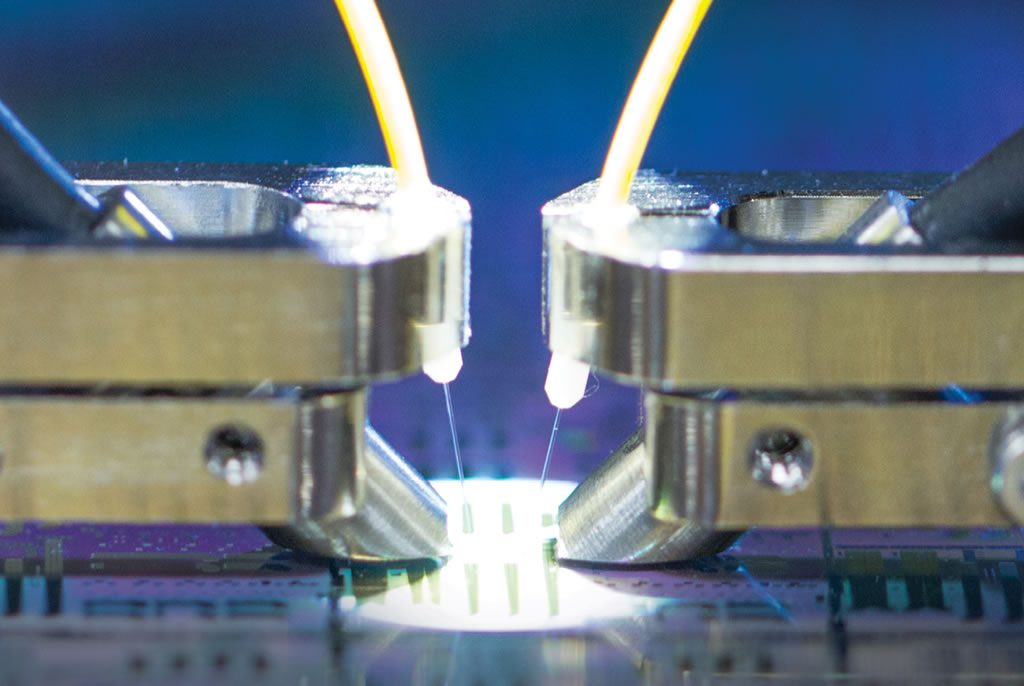
Enabling and Optimizing Optical Coupling for Silicon Photonics
The use of single optical fibers and fiber arrays as probes to couple light into and out of a wafer surface creates many challenges that FormFactor manages through its Contact Intelligence technology. Unlike electrical testing, optical testing uses fibers and fiber arrays that do not contact their corresponding ‘pads’ known as grating couplers on the wafer surface. Instead, fibers need to be articulated above these couplers to find the position of maximum optical power transfer. Setting the initial Z position of the fiber or array tips relative to the wafer surface and then optimizing their position is accomplished through a unique automated technique developed by FormFactor engineers. Using advanced image processing and specially developed algorithms, incident angles and rotational axes can be automatically adjusted and set accordingly.
FormFactor has also implemented a Z displacement sensing technology that enables precise sub-micron level placement accuracy of the fibers and arrays when stepping die-to-die. These automated optical capabilities can also be combined with programmable DC and RF positioning technology to create a truly automated Optical-Optical, Optical-Electrical, and Optical-Electrical-Optical test platform.
For optical applications, Contact Intelligence reduces what used to take days, weeks or months to a matter of minutes while offering flexibility in a dynamic engineering environment and a stable repeatable environment for production.