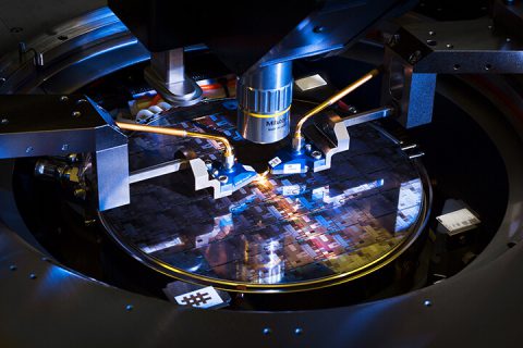
The MicroVac™ chuck is specifically designed for customers who are testing high-power RF amplifiers, typically HEMT devices, operating up to 60 GHz. These high electron mobility transistors are manufactured on III/V compound semiconductor substrates (GaAs or GaN wafers) and are used in various wireless communications products for commercial and military requiring high-power signal transmissions.
Thinned Wafer Testing
These high-power RF devices require wafer thinning before testing and packaging. The thinning process removes excess wafer substrate material below the device, which acts as a thermal insulator, trapping heat, leading to low performance, damaged, or destroyed devices. In the thinning process, wafers can be thinned down to just 50-100 μms, which can cause warping, and sometimes the wafers will crack or break into partial wafers.
Testing Problems with Thinned Devices
Electrical test is usually performed with the thinned wafer on a probe station wafer chuck, before dicing and assembling the device into a package/heat sink. When a thinned wafer is on the chuck, it is critical to have uniform vacuum hold-down across the entire thinned wafer contact area for the following reasons:
- To reduce pad damage / slow test speed. Uneven vacuum hold-down across the wafer causes warped wafers to have varying test pad heights (P-P ~ 50-100 μm). Probe touchdown on the pads can sometimes cause pad damage by excessive overdrive. To compensate for Z height variations, time-consuming wafer profiling must be done, which can increase test time.
- To minimize device damage. Non-uniform vacuum across the wafer causes some areas to have low thermal conductivity to the chuck, so that when the device is electrically tested, the device can overheat, and be damaged or destroyed.
- To obtain highest accuracy / device yield. Similar to number two above, non-uniform vacuum hold-down across the wafer causes non-uniform heat dissipation, which can limit the maximum device performance. Not only does this produce inaccurate data but it can also reduce wafer yield by inaccurately binning device as lower performance than actual performance when packaged.
MicroVac Technology Increases Yield
The patented MicroVac chuck technology provides uniform vacuum across the entire wafer surface. The improved vacuum design minimizes leaks and provides constant vacuum – leading to the best possible thin wafer pull-down performance available on the market. For thinned wafer surfaces, uniform probe overtravel can be achieved at any wafer position resulting in repeatable contact and measurement results.
In addition, the dedicated vacuum design enables easy and quick pull-down of even heavily warped wafers, reducing time to obtain high accuracy data. Wafers can be thinned, warped, or cracked. Even partial wafers (that do not cover all the chuck vacuum holes) are held down with uniform vacuum to achieve maximum device thermal conductivity to the chuck, and uniform Z height.
Key features of the patented MicroVac chuck include:
- 495 micro-holes with 200 µm diameter patterned throughout the chuck
- High-flow internal vacuum channel design
- Gold-plated surface finish
- Five user selectable vacuum zones
What are the resulting customer benefits of this?
- Accurate measurement for lateral high-power RF devices
- Uniform heat conductivity (better DUT statistics)
- Improved thin-wafer handling (uniform overtravel)
- Best warped wafer pull-down (reduces manual adjustments)
When testing high-performance thinned GaAs and GaN wafers, the MicroVac technology enables highest accuracy lateral RF power device performance and yield.
For more information on the MicroVac chuck, please download the Summit™ data sheet or visit our website.