VCSEL and MicroLED Measurements
Optical technologies create new possibilities – securer, safer, and smarter.
Vertical-Cavity Surface-Emitting Lasers (VCSELs)
| New uses for VCSELs in smartphone and automotive applications are continuing to drive the VCSEL market to new heights. 3D sensing for facial recognition is the key application in smartphones with up to three VCSEL dies being integrated into a single smartphone. Emerging automotive applications such as driver monitoring, infotainment control and LiDAR will provide an additional boost to the VCSEL market and sustain its continued growth. As 3D sensing, enabled by VCSELs, continues to find new applications, the technology we use on a regular basis will become securer, safer and smarter. |  |
Micro Light Emitting Diodes (μLEDs)
μLED display technology is drawing increased attention, and μLED displays will arrive soon in consumer products. There are multiple emerging applications for μLED displays such as wearables, smartphones/tablets, TVs, virtual/augmented reality (VR/AR) and automotive. Compared to OLED, LCD and other display technologies, μLED displays have higher resolution, greater dynamic range, faster response, and lower power consumption (for longer battery life).
 |
Challenges of μLED Probing
A major requirement for on-wafer μLED testing is single and dual sided testing which entails probing on one side and optical measurements with an integrating sphere and detector on the other side. The probe system must support thin, warped wafer handling (GaAs, InP, and others, 4” and 6”), as well as probe-to-pad alignment on very small pad/bump sizes and pitches. Finally, the system must deliver fast and efficient production style test of millions of DUTs per wafer with high parallelism and quick/accurate stepping.
Pioneering Tools for VCSEL and μLED Test
Testing optical devices directly on wafer requires sophisticated automated probing solutions. FormFactor addresses these challenges with a range of dedicated manual, semi- and fully automated probe stations for high-precision single and dual sided optical on wafer measurements.

Special Double-Sided Chuck (VCSEL)

For dual sided probing, the wafer is located on the bottom side of the chuck. It is held in place against a glass support via vacuum. This design enables unobstructed probing on the bottom side of the wafer. The transparent glass support allows optical measurements from the top side of the wafer with a triple optic system.
Patented Thermal System Technology (VCSEL)
As there is no thermal chuck possible when probing both sides of the wafer, the measurement setup requires a localized cooling and heating source for accurate cool-to-hot dual sided testing. FormFactor has designed a new, patented, thermally controlled probe unit, FireProbe, that enables test for both high and low temperature with very stable and accurate conditions. Both probe card and probe positioner types can be chosen for this new technology. Our extensive portfolio of high-performance probes suits most requirements.

Triple Optics System (VCSEL)

Triple optics, including LIV (light intensity, current and voltage), near field and far field, can be mounted on top of the prober while probing from the bottom side of the wafer. The double-sided chuck design allows free access to both sides of the wafer. The wafer itself can be fixed by vacuum or mechanically clamped to allow testing to the substrate edge.
Manual or Motorized Positioners
Double-sided probing is enabled by manual or motorized positioners on the bottom side of the wafer.

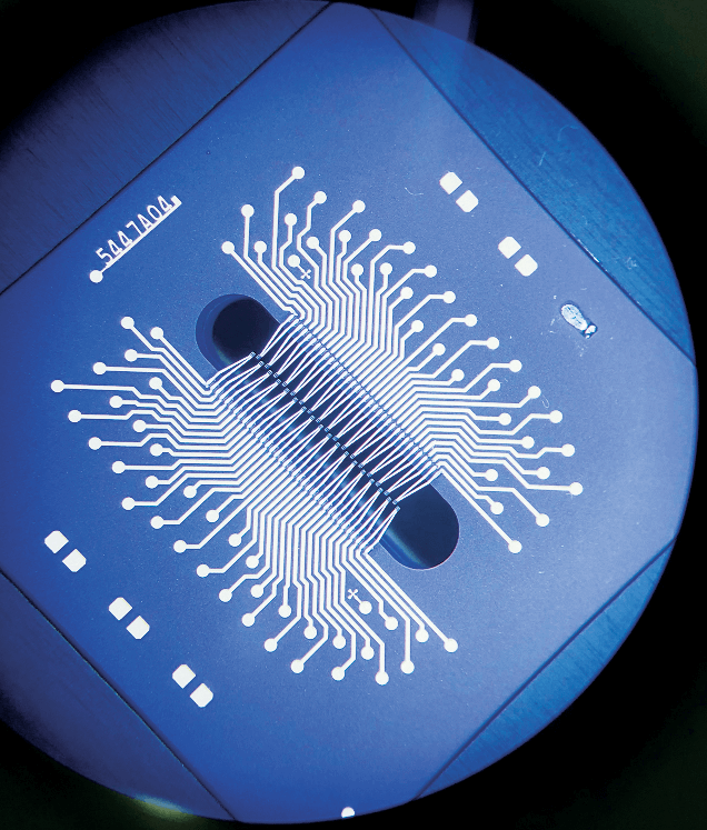
Probe Technology

FormFactor Akari probe cards, with 3D MEMS and 2D MEMS probe options, provide precise probing for electrical signals.
Probe Position Correction (μLED)
A proprietary electrical micro-alignment method augments and enhances FormFactor’s vision-based alignment. This enables fully-auto testing and stepping accuracy of +/-4.5 μm for tight pad/bump pitches with the BlueRay probe system.