Optical Wafer Test
for CIS and LED Devices
The applications for optical data transmission are growing. FormFactor’s family of optical device probe cards offer customized solutions for testing CMOS image sensors and LED devices.
Two popular uses for semiconductors and compound semiconductor materials in the optical device industry are the applications of LED and CMOS image sensor manufacturing. LEDs convert electricity to light by way of semiconductor materials and CMOS image sensors convert light passed through a lens to digital information. The two applications have broadly changed the home and commercial lighting industries, and revolutionized the camera industry in the conversion from analog to digital image capture.
Light Emitting Diodes (LEDs)
With the growing need for energy-saving devices, LED lighting is being widely adopted across the world. LED bulbs generate light by passing an electrical current though a microchip – otherwise known as electroluminescence.
The diode light in LEDs is roughly 75% more efficient than the filament light in incandescent bulbs, making LEDs a favorable choice for illumination. In addition, LEDs emit little heat and have long lifetimes. LEDs are now used in an extensive range of applications, including household lighting, car signals, TVs, billboards, cameras, UVC surface disinfecting lights, and medical devices.
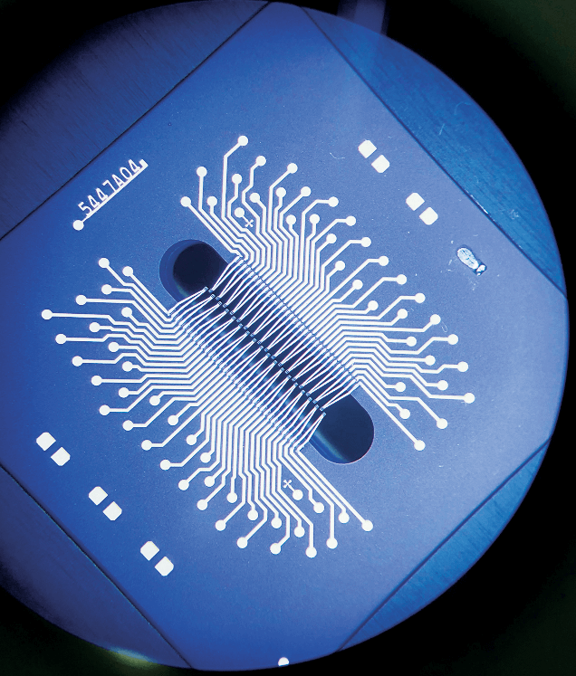
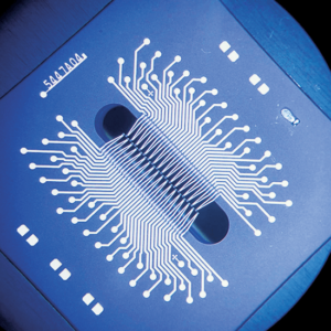
Akari probe cards, with both multi-site and single-site/2-pin options, deliver a high-precision test solution for LEDs. Using FormFactor’s 3D MEMS MicroSpring® technology, Akari provides consistent and small scrub marks for minimal damage on gold pads. With fewer particles generated, Akari probe cards require less maintenance and allow for longer cleaning intervals. Akari’s excellent 3D MEMS spring stability ensures contact accuracy over millions of touchdowns.
Designed for low and stable contact resistance, Akari is optimized to help LED suppliers achieve fewer re-sorts and maximize yields.