October 23, 2026
On the Semiconductor Leadership Podcast, FormFactor CCO Aasutosh Dave explains why the industry must scale capacity and technology together, and why silicon photonics is moving from lab to fab.
October 23, 2026
On the Semiconductor Leadership Podcast, FormFactor CCO Aasutosh Dave explains why the industry must scale capacity and technology together, and why silicon photonics is moving from lab to fab.
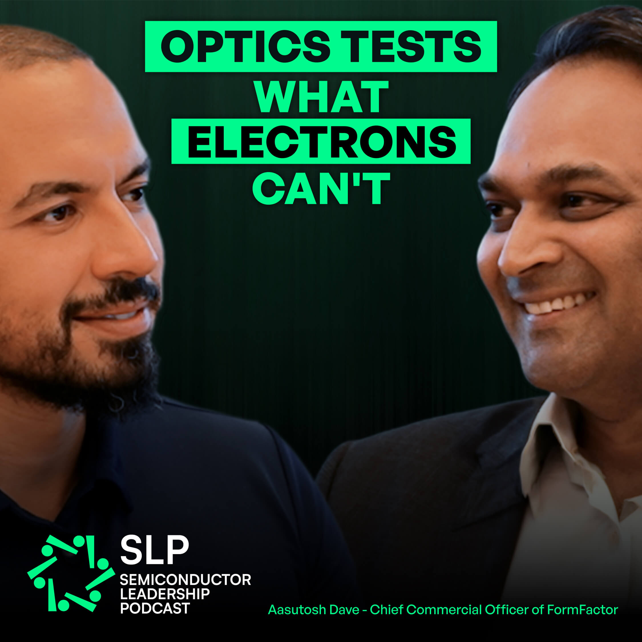
How will semiconductor test keep up as AI drives unprecedented demand? FormFactor Chief Commercial Officer Aasutosh Dave took on that question in a recent episode of the Semiconductor Leadership Podcast with host Salah Nasri. Throughout the conversation, he explored why capacity and technology must scale together, why the entire semiconductor ecosystem must evolve, and how silicon photonics is moving from the lab to high-volume manufacturing.
Aasutosh was direct about the market. “The demand is completely unprecedented, and capacity constraints are real,” he said. But he drew an important line: “Customers are not just looking for capacity. They’re looking for capacity with the right technology.”
That technology is changing fast. Advanced chips are introducing higher current requirements, hybrid and copper bonding, different pad structures, and increasingly complex memory and high-performance computing stacks, creating new test challenges.
One customer summed up the pace in a phrase Aasutosh shared: “We are building the bridge while walking on it.” Keeping up means anticipating technology insertion points while expanding the capacity needed to support customers. The ramp of FormFactor’s new manufacturing facility in Farmers Branch, Texas, is one example.
Ten or fifteen years ago, few customers talked about their test suppliers. That has changed as the cost of test and the cost of yield loss rise. Aasutosh compared today’s back end to front-end manufacturing 10 to 20 years ago, when close engagement and joint development became the norm. “We are no longer a commodity,” he said.
Test is also no longer an isolated step. Probe and interface technology, automated test equipment, and the rest of the test infrastructure must evolve with the devices and packages they serve. “You have to make sure that there is no one bottleneck that fails,” Aasutosh said. That is why FormFactor works with an open ecosystem of partners, including Advantest and Teradyne.
The same thinking shapes FormFactor’s commercial approach. “The sales job is not just to get the PO,” he said. It means partnering with customers across the full product life cycle, starting with their technical challenges.
Asked to name the one shift in semiconductor test that most people are not paying attention to, Aasutosh pointed to silicon photonics.
As data rates become increasingly challenging, optics are moving into the mainstream, creating new requirements for semiconductor test. “Instead of electrons testing the chips, it’s optics testing the chip,” he explained. The goal is still known good die. What changes is the scale: much of this testing has historically taken place in R&D environments, and it is now expanding into high-volume manufacturing.
FormFactor calls this progression “lab to fab.” Years of supporting silicon photonics R&D built the foundation for production. TRITON™, FormFactor’s production-ready silicon photonics test cell, is the result. Developed with Advantest and Tokyo Electron (TEL), it combines optical and electrical test at the wafer level for high-volume manufacturing.
Is that shift still years away? “It’s already happening right now,” Aasutosh said.
The same approach applies to technologies still in research, such as quantum computing: lay the foundation early, work closely with customers, and, in Aasutosh’s words, “when that switch happens, you want to make sure you’re ready.”
He returned often to one principle: curiosity. The industry has repeatedly broken through limits once thought fundamental, and doing it again will take a new generation of engineers. “How many optics engineers do we have?” he asked. His advice to them was simple: always be curious.
Watch the full Semiconductor Leadership Podcast episode with Aasutosh Dave for more on AI-driven demand, advanced packaging, silicon photonics, and leadership in a fast-changing industry.