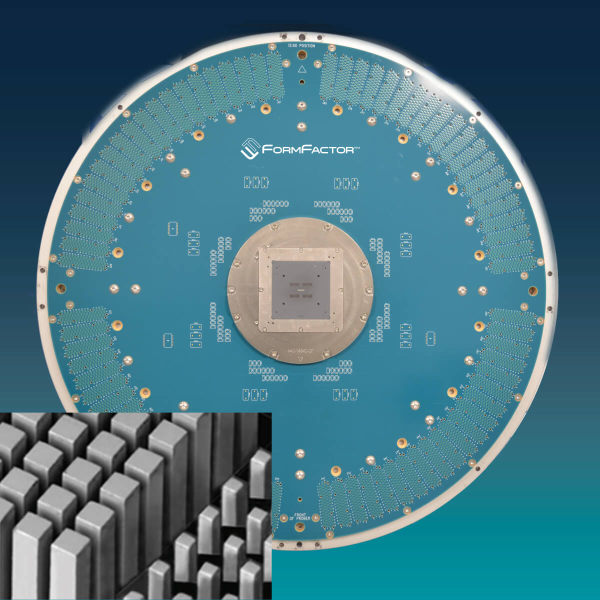
Micro-bump probing has a reputation for being difficult. And to be fair, there are good reasons for that.
As AI accelerators, high-bandwidth memory (HBM), chiplets, and heterogeneous integration architectures become more complex, the bumps are getting smaller, pitches are getting tighter, and test requirements are getting tougher. Advanced packaging platforms such as TSMC CoWoS®, Intel® Foveros™ and EMIB, Samsung advanced packaging technologies, and other 2.5D and 3D integration approaches depend on increasingly dense interconnects.
AI is pushing things even further. GPUs paired with HBM, custom AI accelerators, networking ASICs, and other high-performance devices are putting new demands on both packaging and wafer-level test.
Against that backdrop, it’s easy to understand why some assumptions about micro-bump probing have stuck around. The alignment tolerances are too tight. The probes can’t handle the power. Testing is too expensive. Touching the bumps will damage them.
There’s usually a legitimate engineering concern behind each of these statements. But that doesn’t necessarily make the conclusion true.
Let’s take a closer look at six common micro-bump probing myths and what production experience tells us today.
What Is Micro-Bump Probing, and Why Does It Matter?
Micro-bump probing makes electrical contact with fine-pitch bump structures during wafer test, giving manufacturers an opportunity to characterize devices before they move further into the packaging process.
That opportunity matters more as packages become more complex.
Consider a device that combines multiple dies, HBM stacks, and other components in a single advanced package. Finding out that one of those components has a problem after assembly is very different from finding it earlier in the process. The farther a defective device travels through an expensive manufacturing flow, the more is potentially at stake.
That’s one reason micro-bump testing has attracted so much attention. The question isn’t simply whether engineers can physically make contact with increasingly small bumps. It’s whether they can do it repeatedly, at production scale, without creating another problem somewhere else in the process.
And that’s where some of the conventional wisdom needs updating.
Myth #1: Micro-Bump Probing Is Too Challenging for High-Volume Manufacturing
Let’s start with the obvious: micro-bump probing isn’t easy.
Smaller bumps and tighter pitches leave less room for error. Alignment, contact stability, probe durability, and process consistency all matter. A solution that works a few times in an engineering lab isn’t necessarily ready to run repeatedly in a production environment. But that’s very different from saying micro-bump probing can’t be used in high-volume manufacturing.
Production deployments have demonstrated that it can be done when the probe architecture and process controls are designed around the application. The conversation has therefore shifted from “Can we probe this?” to “What does it take to probe this reliably at scale?”
That’s a much more useful question.
Myth #2: Micro-Bump Probing Is Only Available Through Foundry Test Services
This assumption made more sense when micro-bump probing was less mature and there were fewer options available. That’s changing.
As advanced packaging adoption has grown, semiconductor manufacturers have more ways to think about where micro-bump testing fits into development and production. Instead of assuming the capability has to remain within a specialized foundry test service, manufacturers can evaluate test strategies based on their own devices, processes, volumes, and business requirements.
That flexibility becomes increasingly important as AI, HBM, and chiplet volumes grow. Different manufacturers may have very different priorities around test coverage, throughput, cost, and control of the test process.
There isn’t one micro-bump test strategy that makes sense for everyone.
Myth #3: Micro-Bump Test Insertion Is Always Too Expensive
This concern is understandable. Adding another test insertion sounds like adding cost. Sometimes it does.
But focusing only on the cost of the test step misses a larger question: What does it cost to discover a problem later?
With advanced packaging, multiple valuable components may eventually come together in the same package. Finding a defective component after more processing and assembly have taken place can carry a very different economic impact than identifying it earlier.
That doesn’t mean more testing is always better. Engineers still need to make choices about coverage, throughput, parallelism, insertion points, and the amount of data they actually need. The real goal is to find the right balance.
A well-designed strategy looks at the economics of the entire manufacturing flow rather than treating micro-bump probing as an isolated expense. In some applications, more test may make sense. In others, a more targeted approach may be the better answer.
Myth #4: Fine-Pitch Micro-Bumps Require Impossible Alignment Accuracy
It’s easy to see where this assumption comes from. If bumps keep getting smaller and closer together, the allowable alignment error must eventually become impossibly small, right? Not necessarily.
Alignment is important, but it isn’t the only factor determining whether reliable contact can be made. Probe tip geometry, bump geometry, contact mechanics, process control, and the overall probe architecture all influence the available contact window.
In other words, looking at alignment accuracy by itself doesn’t tell the whole story.
The practical question is whether the complete probing system can repeatedly make good electrical contact within the process window available for that particular device.
Production experience shows that the answer can be yes, even at pitches that might initially make engineers skeptical.
Myth #5: Power Requirements Exceed What Micro-Bump Probes Can Handle
This one is becoming particularly important for AI and HPC devices.
These devices can have demanding power requirements, and asking a fine-pitch probe architecture to deliver substantial current raises legitimate concerns. Contact resistance, current distribution, thermal behavior, and probe robustness all come into play.
But again, the challenge shouldn’t be confused with an absolute limit. Probe architectures and power delivery strategies have evolved alongside the devices they’re being asked to test. The right approach depends on the actual requirements of the DUT, including how current needs to be distributed and how the probing system behaves electrically and thermally under load.
There isn’t a magic probe that makes power delivery irrelevant. There are, however, engineering approaches for dealing with it. That’s an important distinction.
Myth #6: Probing Damages Micro-Bumps and Creates Reliability Risks
This may be the concern engineers raise most often, and it’s probably the one that deserves the most careful answer.
Yes, probing involves physical contact. And yes, that contact can leave a mark or create some amount of deformation. The important question is what happens next.
Not every visible probe mark creates a reliability problem. What matters is whether the interaction between the probe and bump stays within a characterized process window that is compatible with downstream assembly.
That means looking at factors such as probe tip geometry, contact force, bump material and structure, overtravel, deformation, and the requirements of the subsequent packaging process.
This is why characterization matters so much. Engineers need to understand not just whether they can establish electrical contact, but what that contact does to the bump.
The goal isn’t a bump that looks untouched. The goal is repeatable electrical contact without compromising downstream manufacturing or package reliability.
What Should Engineers Take Away from These Micro-Bump Probing Myths?
Micro-bump probing still presents real engineering challenges. Pretending otherwise wouldn’t be particularly helpful.
But many of the assumptions surrounding alignment, cost, power handling, and reliability were formed when the technology and manufacturing ecosystem looked very different.
Today’s question isn’t whether micro-bump probing is difficult. It is. The better question is whether those challenges can be understood, characterized, and controlled well enough to support a practical manufacturing process.
Increasingly, production experience says they can. For engineers developing test strategies for AI, HBM, chiplets, HPC, networking, and other advanced packaging applications, that means it’s worth revisiting assumptions that may have been formed several technology generations ago.
Look at the device. Look at the process window. Look at where test adds value. And then make the decision based on actual application requirements and production data rather than conventional wisdom.
Want to Put These Micro-Bump Myths to the Test?
How much alignment margin do you really need? Should micro-bumps be tested before or after reflow? Which probe tip geometry provides the best contact performance? How much bump deformation is acceptable?
Those are the kinds of questions that are difficult to answer with rules of thumb alone.
In the on-demand webinar, “Breaking Down Micro-Bump Probing Myths,” Alan Liao, Director, Probe BU Product Marketing, and Jeremy Streifer, Technical Director, Development Engineering, dig into these questions using real-world production examples and application data.
Watch the webinar to learn more about:
- Micro-bump alignment requirements
- Native-pitch versus relaxed-pitch probing strategies
- Probe tip geometry and contact optimization
- Power delivery and probe robustness
- Bump deformation and reliability
- Test strategies for AI, HBM, HPC, and advanced packaging applications
Watch the webinar to find out which micro-bump probing assumptions still hold up and which ones are ready to be retired.
FAQs – Micro-Bump Probing
What is micro-bump probing?
Micro-bump probing is a wafer-level test technique that makes electrical contact with fine-pitch micro-bumps before advanced packaging or assembly. It allows engineers to characterize device performance and potentially identify problems earlier in the manufacturing process.
Why is micro-bump probing important for HBM and AI devices?
HBM, GPUs, AI accelerators, and other high-performance devices increasingly rely on advanced packages containing multiple components and dense interconnects. Micro-bump probing can provide electrical test data before those components move farther into complex and costly packaging processes.
Can micro-bump probing be used in high-volume manufacturing?
Yes. Micro-bump probing can be used in high-volume manufacturing when probe technology, contact mechanics, alignment, test architecture, and process controls are designed around the specific application. The challenge is achieving repeatable performance at production scale rather than simply demonstrating that contact is possible.
How accurate does alignment need to be for micro-bump probing?
There isn’t one alignment specification that applies to every device. Bump size and pitch matter, but so do probe tip geometry, contact mechanics, process control, and the overall probing architecture. Engineers need to evaluate the complete contact window for the application.
Does probing damage micro-bumps?
Probing can leave contact marks or cause some deformation. That does not automatically mean the bump has been damaged in a way that affects reliability. The key is understanding how much deformation occurs and whether it remains within a qualified process window for downstream assembly.
Can micro-bump probes handle the power requirements of AI and HPC devices?
They can be designed for demanding power requirements, but current delivery needs to be considered as part of the overall test architecture. Contact resistance, current distribution, probe robustness, and thermal behavior all need to be evaluated against the requirements of the device.
Is micro-bump testing expensive?
It can add test cost, but that’s only part of the equation. Manufacturers also need to consider the value of identifying defective devices earlier, before additional processing and packaging costs have been added. The most effective strategy balances test coverage, throughput, cost, yield, and the economics of the complete manufacturing flow.