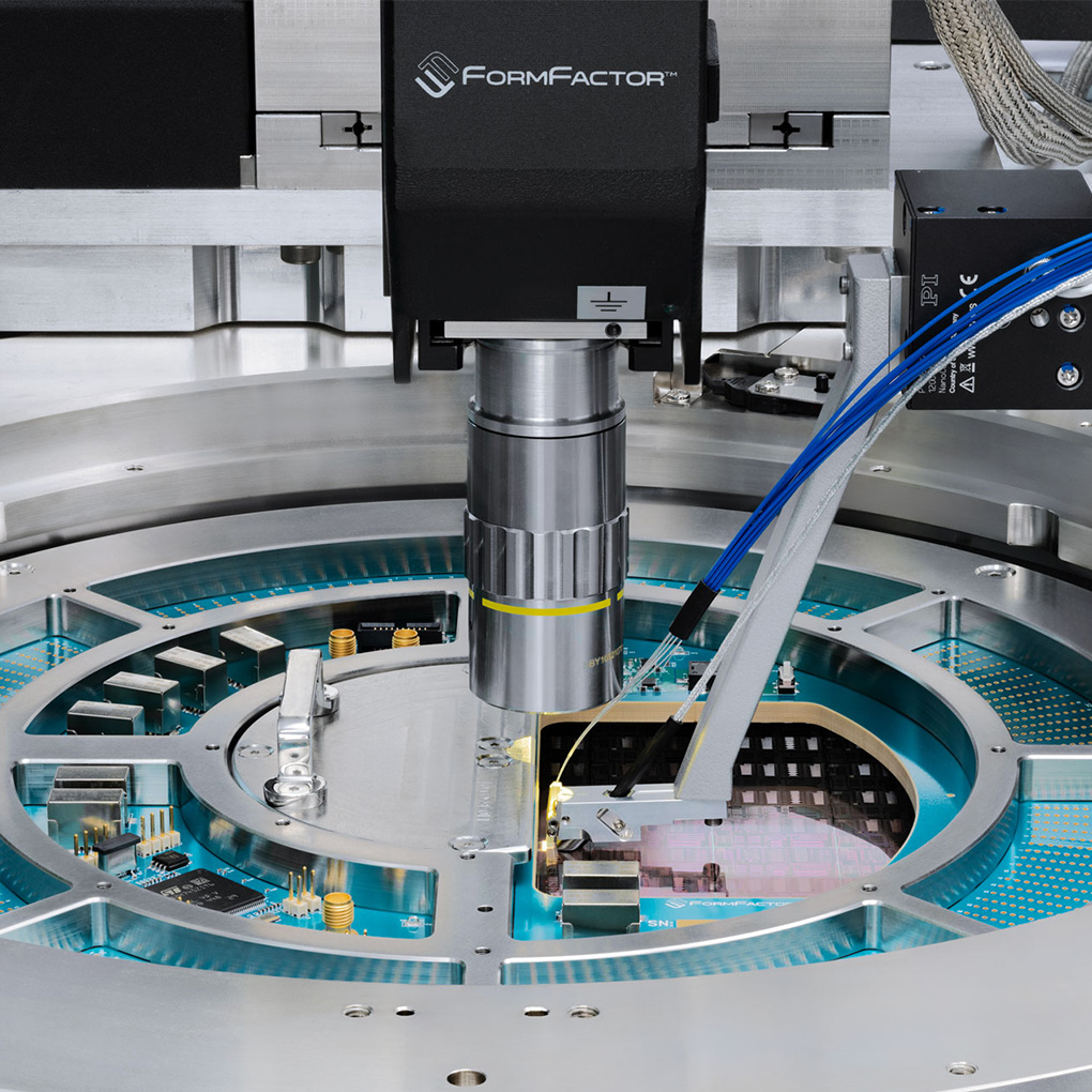
Artificial intelligence is changing the economics of data centers, and silicon photonics is quickly becoming one of the enabling technologies behind that transformation. As data rates climb beyond 800G and the industry looks toward 1.6T optical interconnects, traditional electrical connections alone are no longer sufficient to move massive amounts of data efficiently.
Designing photonic integrated circuits (PICs) is only part of the challenge. Before those devices ever make it into production, manufacturers have to prove they perform exactly as intended. That’s where silicon photonics testing comes in. It has become one of the most important steps in moving these increasingly complex devices from development into manufacturing.
What is silicon photonics testing?
Silicon photonics testing is the process of electrically and optically characterizing photonic integrated circuits during research, development, and wafer-level manufacturing. It combines traditional semiconductor probing with precision optical alignment to verify device performance before packaging, helping engineers improve yield, validate designs, and accelerate production.
As silicon photonics moves from research labs into high-volume manufacturing, testing must become faster, more repeatable, and increasingly automated.
Why silicon photonics testing is more challenging than traditional wafer test
Conventional semiconductor devices primarily rely on electrical signals. Silicon photonics devices combine electrical circuitry with optical waveguides, modulators, detectors, lasers, and fiber interfaces on a single chip, and that creates an entirely different set of measurement challenges.
During silicon photonics wafer testing, engineers often need to:
- Measure optical insertion loss
- Characterize wavelength response
- Validate electro-optical modulation
- Verify optical power levels
- Test high-speed electrical interfaces
- Measure thermal behavior
- Confirm device repeatability
Meeting these requirements depends on advanced probe systems that can integrate precision motion, optical alignment, electrical probing, thermal control, and automation into a single test environment.
Even tiny positional changes can significantly affect measurement accuracy.
Challenge 1: Optical alignment at the micron level
Perhaps the greatest challenge in silicon photonics testing is optical alignment. Unlike traditional electrical probing, where probe needles simply contact metal pads, photonic testing requires light to be coupled efficiently into microscopic waveguides.
Alignment tolerances are often measured in microns, and in some applications sub-microns, leaving very little room for variation. Engineers must position optical fibers with sub-micron accuracy while maintaining stable coupling throughout the measurement process. Any vibration, drift, or thermal expansion can change optical coupling efficiency and produce inconsistent results.
In fact, FormFactor recently demonstrated how automated optical alignment significantly improved silicon photonics testing efficiency through its collaboration with IHP, highlighting the growing importance of automation as photonic devices become more complex.
Challenge 2: Simultaneous electrical and optical measurements
Silicon photonics testing requires engineers to evaluate both the electrical and optical behavior of a device at the same time.
Electrical probing verifies:
- Power delivery
- Signal integrity
- Device functionality
- High-speed interfaces
Optical characterization measures:
- Optical loss
- Laser performance
- Modulation efficiency
- Wavelength response
- Fiber coupling efficiency
Collecting these measurements independently can dramatically increase test time and introduce additional variability.
Modern integrated photonics test solutions instead coordinate both measurement environments within a single automated workflow, allowing engineers to collect more comprehensive data while reducing overall test complexity.
Challenge 3: Throughput for high-volume manufacturing
Spending several minutes characterizing a single device may be acceptable in the lab, but that approach doesn’t scale once production begins.
As silicon photonics adoption accelerates across AI infrastructure, cloud computing, co-packaged optics, and high-speed networking, manufacturers must test significantly more devices while maintaining measurement quality.
High-volume silicon photonics testing requires automated wafer handling, repeatable optical alignment, efficient measurement sequences, and software-controlled workflows that can keep pace with production demands. Automation reduces operator variability while dramatically increasing throughput. The TRITON system is made for these challenges.
Challenge 4: Measurement repeatability
Consistent measurements are essential in semiconductor manufacturing because every production decision depends on trusting the data.
Engineers need confidence that today’s measurements will match tomorrow’s measurements regardless of operator, shift, or location.
Several factors can introduce variability during silicon photonics wafer probe testing, including mechanical vibration, temperature fluctuations, probe wear, fiber alignment drift, and inconsistent electrical contact.
Automated systems minimize these variables by using programmable positioning, repeatable alignment algorithms, and standardized measurement workflows. The result is greater confidence in characterization data and improved measurement consistency.
Challenge 5: Thermal effects
Temperature influences nearly every aspect of photonic device performance.
Changes in temperature can affect:
- Laser wavelength
- Optical loss
- Modulator efficiency
- Detector sensitivity
- Electrical performance
Many applications require characterization across a wide temperature range to understand how devices will behave under real operating conditions.
Integrating thermal control into silicon photonics wafer-level testing allows engineers to evaluate performance across those conditions while maintaining stable optical alignment throughout the test process.
Challenge 6: Scaling from development to production
Many silicon photonics devices begin life in research laboratories, where engineers have the flexibility to use manual alignment, custom scripts, and specialized measurement setups. Manufacturing places a very different set of demands on the test process.
Production environments require standardized workflows, automated alignment, high repeatability, fast cycle times, and minimal operator intervention. Successfully transitioning from R&D characterization to production testing requires equipment that can support both environments without compromising measurement accuracy.
Automation Is Changing Silicon Photonics Testing
As silicon photonics moves from research into high-volume manufacturing, manual testing quickly becomes a bottleneck. Engineers still need the same level of precision, but they also need to characterize far more devices in far less time without sacrificing measurement quality. Automated silicon photonics systems, such as FormFactor’s Autonomous Silicon Photonics platform, help address these challenges by streamlining optical alignment and improving measurement consistency.
Today’s advanced probe stations combine high-precision wafer positioning, optical fiber alignment, electrical probing, temperature control, motion control, and automated measurement software into a single platform. Instead of relying on manual alignment and operator intervention at every step, these systems can automatically locate devices, align optical fibers, execute repeatable test routines, and collect both electrical and optical measurements with consistent accuracy.
The benefits extend well beyond faster testing. Automation helps reduce operator-to-operator variability, improves measurement repeatability, and makes it easier to transition proven test methods from R&D into production. It also allows engineering teams to scale manufacturing without relying on increasingly scarce photonics specialists to perform every measurement manually.
As silicon photonics devices continue to grow in complexity, integrating automation into the probe station is becoming one of the most effective ways to improve throughput while maintaining the precision required for next-generation photonic integrated circuits.
Looking ahead
Silicon photonics is rapidly becoming a foundational technology for AI infrastructure, hyperscale data centers, telecommunications, and advanced computing.
As device complexity increases, testing will continue to play a larger role in determining manufacturing yield, production efficiency, and overall device performance.
Manufacturers that successfully scale silicon photonics production will be those that can combine precise optical alignment, accurate electrical measurements, automation, and repeatable wafer-level characterization into a single integrated workflow.
FormFactor’s automated silicon photonics solutions are designed to help engineers meet these challenges by enabling faster characterization, improved repeatability, and scalable wafer-level testing for both research and production environments.
Whether supporting early-stage photonic integrated circuit development or high-volume manufacturing, advanced silicon photonics testing helps ensure that next-generation optical technologies can move efficiently and confidently from the lab to the fab.
FAQs – Silicon Photonics Testing
What is silicon photonics testing?
Silicon photonics testing is the process of measuring the electrical and optical performance of photonic integrated circuits (PICs). Engineers perform wafer-level testing to verify that devices meet performance specifications before packaging, helping improve manufacturing yield, device reliability, and overall production efficiency.
Why is optical alignment so important in silicon photonics testing?
Optical alignment is critical because even microscopic positioning errors between an optical fiber and a photonic device can significantly affect measurement accuracy. Precise, repeatable alignment ensures consistent optical coupling, reliable test results, and accurate characterization throughout the wafer test process.
How is silicon photonics testing different from traditional semiconductor testing?
Traditional semiconductor testing focuses primarily on electrical measurements. Silicon photonics testing requires engineers to evaluate both electrical and optical performance simultaneously, combining precision electrical probing with optical alignment and electro-optical characterization to fully validate device functionality.
What equipment is used for silicon photonics wafer-level testing?
Silicon photonics testing typically uses advanced probe stations equipped with high-precision wafer positioning, optical fiber alignment systems, electrical probes, temperature control, motion control, and integrated measurement software. Automated systems help improve repeatability, reduce test time, and support both research and high-volume manufacturing.
Why is automation becoming more important in silicon photonics testing?
As silicon photonics moves into large-scale production, manual testing becomes too slow and difficult to scale. Automated testing systems improve throughput by reducing alignment time, minimizing operator variability, executing repeatable test sequences, and maintaining consistent measurement quality across thousands of devices.
What industries benefit from silicon photonics testing?
Silicon photonics testing supports a wide range of industries, including AI infrastructure, hyperscale data centers, telecommunications, high-performance computing, and advanced networking. Accurate wafer-level testing helps manufacturers deliver reliable optical devices that enable faster data transmission, lower power consumption, and higher system performance.