For years, evaluating a probe was fairly straightforward. If it delivered reliable contact, held up over time, and supported good production yield, it was doing its job.
That assumption is changing, however.
As semiconductor devices for high-speed interconnection and networking moves from 112G to 224G and begin planning for 448G, vertical probes is no longer just connecting the tester to the device. They have become an active part of the measurement system. Their electrical and mechanical design now has a more direct and measurable impact on signal integrity, measurement margin, and how much confidence engineers can have in the results they see.
That shift is happening because AI infrastructure is pushing every part of the interconnect ecosystem toward higher speeds, more current, and much tighter signal margins. These challenges and the technologies addressing them will be the focus of FormFactor’s upcoming webinar, Is Your Probe Closing the Eye? Evaluating Wafer-Probe Performance for 224G and 448G, where experts will discuss the architectural considerations required for reliable high-speed SerDes wafer test.
AI Infrastructure Is Driving New Wafer Test Requirements
The rapid growth of AI is accelerating nearly every high-speed interconnect technology in modern semiconductor design.
Today’s devices rely on increasingly demanding interfaces, including:
- UCIe and Chiplet interconnects
- PCIe and CXL
- NVLink and UALink for GPU-to-GPU communication
- Ethernet and Infiniband for Scale-out networking
- Optical-to-electrical interfaces
Every new generation delivers more bandwidth but leaves engineers with less room for error. The industry has already transitioned from 112G to 224G, and work toward 448G is underway. At these speeds, maintaining signal integrity throughout the entire measurement path becomes significantly more challenging.
More Bandwidth. More Power. Smaller Margins.
Moving from 112G to 224G is far more than doubling data rates.
Higher-speed PAM-4 signaling introduces tighter timing requirements and much less tolerance for signal degradation. At the same time, advanced processors continue demanding higher current delivery through increasingly dense probe arrays.
That leaves engineers trying to solve several difficult problems at once.
They must simultaneously:
- Preserve signal integrity
- Deliver higher current through thousands of contacts
- Maintain consistent mechanical performance
- Minimize measurement uncertainty
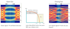
Sources of loss that barely mattered a few years ago can now have a noticeable impact on channel performance. When margins become this thin, every element in the signal path matters.
When Test Results Become Difficult to Trust
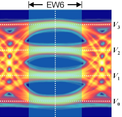
One of the toughest parts of testing at 224G is figuring out whether an unexpected result is coming from the device itself or from the test interface.
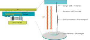
Vertical probes used in the past have electrical paths that are comparable in size to the wavelength of the signal they carry, introducing higher:
- Insertion loss
- Signal reflections
- Crosstalk
- Impedance discontinuities
- Additional variability
That uncertainty slows development down. As eye diagrams begin to close and channel performance falls, engineers have to determine whether the device under test is responsible or whether the measurement system is influencing the result.
Instead of solving the real problem, engineering teams can end up spending days chasing false failures, repeating measurements, or delaying qualification while they figure out what’s causing the issue.
Why Probe Architecture Matters More Than Ever
Historically, many engineers evaluated probe technologies primarily by bandwidth specifications. Today, that is only part of the story.
The way a probe is designed can have a big impact on how consistently measurements are made across thousands of contacts. Factors such as signal path length, mechanical precision, contact behavior, and current-carrying capability all contribute to repeatable high-speed testing.
Engineers are paying closer attention to design characteristics such as:
- Controlled signal paths
- Consistent, high-precision probe geometry
- Stable contact resistance
- Repeatable touchdown behavior
- Scalability across dense arrays
As devices become more complex and pin counts continue to grow, these design details become much harder to ignore.
Five Questions Every Engineer Should Ask About High-Speed Probe Technology
As wafer test requirements continue evolving, evaluating probe technology requires looking beyond headline specifications.
Consider asking these five questions:
- Is the signal path tightly controlled?
Consistent geometry and lithographically-defined precision help reduce electrical variability and improve measurement repeatability.
- Is performance backed by measured data?
S-parameters, channel simulations, and measured results provide valuable, early insight into how the probe will likely behave under realistic operating conditions.
- Does contact resistance remain stable over time?
Stable contact behavior supports both production yield and confidence in measurement consistency.
- Can the probe support increasing current requirements?
Modern AI devices require higher current delivery without excessive force, scrub, or localized heating to minimize the risk of burning the probes.
- Can the architecture scale to dense production arrays?
A probe that performs well in a validation environment must also maintain consistent planarity, alignment, variability, and field maintainability across thousands of touchdowns in high-volume manufacturing.
Asking these questions helps separate marketing claims from measurable engineering data.
Preparing for the Move to 448G
While many companies are just beginning to deploy 224G, the industry is already looking ahead to 448G.
Moving to 448G will leave even less measurement margin and place even greater demands on every part of the test system.
Future probe technologies will need to balance:
- Signal integrity
- Mechanical precision
- Contact stability
- High current delivery
- Manufacturing scalability
As speeds continue to climb, reducing uncertainty throughout the measurement path will become just as important as improving the performance of the device itself.
Learn More During Our Upcoming Webinar
High-speed digital interfaces are evolving quickly, and wafer test strategies have to evolve with them. Engineers need new ways to evaluate probe technologies and ensure the measurement system is delivering results they can trust.
Join FormFactor’s upcoming webinar, Is Your Probe Closing the Eye? Evaluating Wafer-Probe Performance for 224G and 448G, to learn how probe architecture influences signal integrity, measurement margin, and production readiness at today’s highest SerDes speeds. During the webinar, our experts will discuss what changes at 224G, why probe architecture matters more than ever, and what engineers should look for as they prepare for 448G and future high-speed designs.
Register today at the link above to discover how reducing uncertainty in the measurement path can help accelerate development, improve confidence in wafer test results, and prepare your organization for the next generation of semiconductor devices.