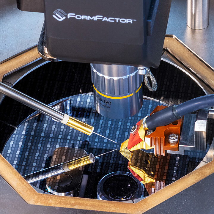
As power semiconductor devices move toward higher voltages and wider-bandgap materials such as silicon carbide (SiC) and gallium nitride (GaN), wafer-level characterization is becoming more demanding. Engineers need to apply increasingly high voltages while still making accurate measurements of leakage current, breakdown voltage, and other critical device parameters.
A high-voltage probe(opens in new tab) is an important part of that measurement environment. Choosing one based on voltage rating alone can create problems ranging from excessive leakage and measurement instability to arcing and premature device failure.
For wafer test, handling the required voltage is only part of the job. Leakage, probe geometry, guarding, contact quality, and the test environment can all affect the measurement, and they need to work together.
Here are eight important considerations when selecting a high-voltage probe for wafer-level testing.
What Is a High-Voltage Probe for Wafer Test?
A high-voltage probe provides the electrical connection between test instrumentation and a device under test (DUT) while supporting voltages beyond those typically handled by conventional wafer probes.
In power semiconductor characterization, high-voltage probes may be used for measurements such as device breakdown, leakage current, and other DC electrical characteristics. Because these measurements can involve both high electric fields and very small currents, the probe must provide reliable electrical contact without introducing unwanted leakage or instability into the measurement.
That makes high-voltage wafer probing(opens in new tab) fundamentally different from simply connecting a high-voltage test lead to a packaged device. At wafer level, probe tips, pads, neighboring structures, chuck surfaces, cables, connectors, and even environmental conditions can influence the measurement.
That’s why it makes sense to look at high-voltage testing as a complete measurement system, rather than focusing on the probe alone.
1) Start With the Required Voltage Range
The first specification most engineers look at is maximum voltage, and for good reason. A high-voltage test probe must be designed to safely support the voltage required by the device and test procedure.
But selecting a probe rated for the DUT’s nominal operating voltage may not be enough. Characterization often requires testing beyond normal operating conditions to understand breakdown behavior or establish device margins. Engineers should consider the maximum voltage that may be applied during the entire test sequence rather than only the expected operating voltage.
For devices that require measurements into the kilovolt range, this may mean selecting a probe specifically designed for several kilovolts rather than adapting a conventional DC probe.
FormFactor’s High Voltage Probes are designed for high-voltage wafer probing applications, providing a solution for measurements where voltage capability, low leakage, and controlled probing conditions are critical. Voltage rating is a good place to start, but it shouldn’t be the deciding factor.
2) Pay Close Attention to Leakage Current
One of the biggest challenges in high-voltage wafer testing is distinguishing current flowing through the DUT from current taking another path through the measurement system.
This is especially important when measuring devices that are expected to exhibit extremely low leakage. Leakage can occur through multiple paths, including the probe itself, cabling and connectors, the probe station, contaminated surfaces, or the surrounding environment. At sufficiently high voltages, even leakage paths that appear insignificant under normal conditions can affect measurement results.
The result can be misleading data. A device may appear to have higher leakage than it actually does, or measurements may become unstable and difficult to reproduce.
When comparing high-voltage probes, look at leakage performance under real test conditions, not just the maximum voltage on the datasheet.
3) Consider Guarding as Part of the Measurement Strategy
Guarding is another important consideration when measuring small currents at high voltage. A properly designed guard helps control unwanted leakage paths by maintaining surrounding conductive surfaces at an appropriate electrical potential. Instead of allowing stray current to flow into the measurement node, guarding can redirect that current away from the sensitive measurement path.
This can be especially valuable when the current being measured is very small relative to the voltage applied.
But guarding should not be considered a probe-only feature. Effective guarding depends on the complete measurement chain, including the probe, cables, instrumentation, chuck, probe station, and DUT configuration.
So rather than asking only whether a probe supports guarding, consider how it fits into the guarding strategy for the entire measurement setup.
4) Evaluate Probe Tip and Contact Geometry
Mechanical contact is easy to overlook when selecting a high-voltage probe, but it can have a direct impact on measurement quality.
Probe geometry needs to match the device’s pad dimensions, layout, material, and expected probing conditions. The probe needs to establish consistent electrical contact without causing unnecessary pad damage or creating mechanical instability.
High-voltage applications introduce another consideration: electric field concentration. Sharp conductive features and closely spaced structures can create areas of concentrated electric field. At higher voltages, those fields can increase the possibility of discharge or arcing.
Probe design and placement therefore become part of the electrical test strategy. Engineers need to consider probe-tip geometry, spacing between probes, proximity to neighboring structures, and clearance from other conductive surfaces.
Making contact with the pad is only the first step. That contact also needs to remain stable and predictable across the full voltage range of the test.
5) Account for Arcing and Electrical Clearance
As test voltage increases, electrical clearance becomes increasingly important. Arcing can occur when the electric field between two conductive points becomes strong enough to cause electrical breakdown through the surrounding medium. In a wafer probing environment, potential paths can exist between probes, between a probe and the chuck, or between other conductive structures in the test setup.
That makes the physical setup around the DUT just as important as the voltage rating on the probe datasheet.
Probe spacing, chuck configuration, shielding, environmental conditions, and nearby conductive components can all affect high-voltage performance.
The challenge grows as device structures get smaller and contacts move closer together. Semiconductor scaling can push contacts closer together at the same time that power devices require increasingly demanding voltage conditions.
6) Don’t Ignore the Test Environment
Environmental conditions can have a significant effect on high-voltage measurements. Humidity, surface contamination, particulates, and residues can create additional leakage paths. At lower voltages, their effect may be small enough to overlook. During sensitive high-voltage measurements, however, they can become significant sources of measurement error.
Temperature adds another variable. Power semiconductor devices are often characterized across temperature to understand how their electrical behavior changes under different operating conditions. That means the probe and surrounding measurement system may need to maintain stable performance as temperature changes.
For temperature-dependent measurements, the probe and probe station need to be considered together. Both have to remain stable across the intended test conditions.
7) Think About Repeatability, Not Just a Successful Measurement
Getting one good measurement is not the same as having a reliable test process. Device characterization and wafer-level test often require hundreds or thousands of measurements across multiple devices, wafers, temperatures, and operating conditions. Small variations in probe contact, positioning, leakage, or environmental conditions can quickly become significant.
That makes repeatability an important part of choosing a probe. Engineers should consider whether the probe can maintain consistent electrical and mechanical performance through repeated touchdowns and whether its design supports the stability required by the overall test methodology.
This matters even more when moving from engineering characterization toward automated or higher-volume wafer test.
8) Match the Probe to the Complete Power Test Requirement
High voltage is only one dimension of power semiconductor testing. Depending on the application, engineers may also need to perform high-current measurements or characterize devices under combinations of voltage, current, and temperature.
This is where it becomes important to distinguish between a high-voltage probe and a broader high-power probing solution.
A device may require high-voltage testing in its off-state and high-current characterization in its on-state. One probe configuration may not be the best answer for every measurement.
Before selecting a probe, define the complete test envelope:
- Maximum voltage
- Maximum current
- Expected leakage-current range
- DUT pad size and geometry
- Required probe spacing and electrical clearance
- Temperature range
- Guarding requirements
- Measurement instrumentation
- Manual versus automated probing requirements
Once those requirements are clear, it becomes much easier to determine the appropriate probe architecture.
For applications requiring more demanding combinations of voltage and current, FormFactor also offers Ultra-High-Power probing solutions(opens in new tab) designed for power semiconductor characterization.
High-Voltage Probe Selection Is a System-Level Decision
No single specification can tell you whether a high-voltage probe is right for your application.
A 10 kV rating, for example, tells you something important about a probe’s capabilities, but it does not tell you whether that probe will deliver the measurement performance your particular DUT requires.
The probe has to work as part of a larger system that includes the DUT, probe station, instrumentation, cabling, chuck, thermal environment, and test methodology.
That system-level view matters even more as SiC, GaN, and other power semiconductor technologies push wafer-level testing to higher voltages and tighter measurement requirements.
Choosing the Right High-Voltage Probe
When choosing a high-voltage probe, start with the electrical requirements, but look beyond the voltage rating. Leakage, guarding, contact geometry, electrical clearance, temperature, and repeatability all play a role in the quality of the measurement.
Just as important, consider how the probe will work with the rest of the test setup. The probe station, instrumentation, cabling, chuck, DUT layout, and test environment can all influence high-voltage measurements. Looking at the complete system helps engineers build a setup that produces accurate, repeatable data as power semiconductor devices continue to push toward higher voltages and more demanding operating conditions.
FAQs – High-Voltage Probes for Wafer Test
What is a high-voltage probe for wafer test?
A high-voltage probe creates the electrical connection between test instrumentation and a semiconductor device on the wafer while supporting voltages beyond those typically handled by conventional DC probes. These probes are commonly used for power semiconductor characterization, including breakdown voltage and leakage-current measurements.
How do I choose the right high-voltage probe?
Start with the maximum voltage and current required by the DUT, but don’t make the decision based on voltage rating alone. Leakage performance, guarding, probe-tip geometry, electrical clearance, temperature range, pad dimensions, instrumentation, and measurement repeatability should all be considered.
Why is low leakage important in a high-voltage probe?
When measuring very small device currents, unwanted leakage through the probe or other parts of the test setup can become part of the measurement. This can make the DUT appear to have higher leakage than it actually does. A probe and measurement system designed to minimize leakage can improve measurement accuracy and repeatability.
What is guarding in high-voltage wafer testing?
Guarding is a technique used to control unwanted leakage paths around sensitive measurement nodes. A properly designed guard can redirect stray current away from the measurement path. Effective guarding typically involves more than the probe itself and should be considered across the probe, cables, instrumentation, chuck, and probe station.
What causes arcing during high-voltage wafer probing?
Arcing can occur when the electric field between conductive points becomes strong enough to cause electrical breakdown through the surrounding medium. Probe spacing, tip geometry, nearby conductive surfaces, chuck configuration, contamination, and environmental conditions can all influence the risk of arcing.
Can the same probe be used for both high-voltage and high-current wafer testing?
Not necessarily. A device may require high-voltage measurements in its off-state and high-current measurements in its on-state, and the ideal probe configuration for one measurement may not be the best choice for the other. The complete voltage, current, thermal, and measurement requirements should be defined before selecting the probe architecture.
Why does the probe station matter when choosing a high-voltage probe?
The probe does not operate in isolation. Chuck design, probe placement, cabling, shielding, guarding, temperature, environmental conditions, and other elements of the probe station can affect leakage, arcing, and measurement repeatability. For demanding high-voltage measurements, the probe and probe station should be evaluated as parts of the same measurement system.