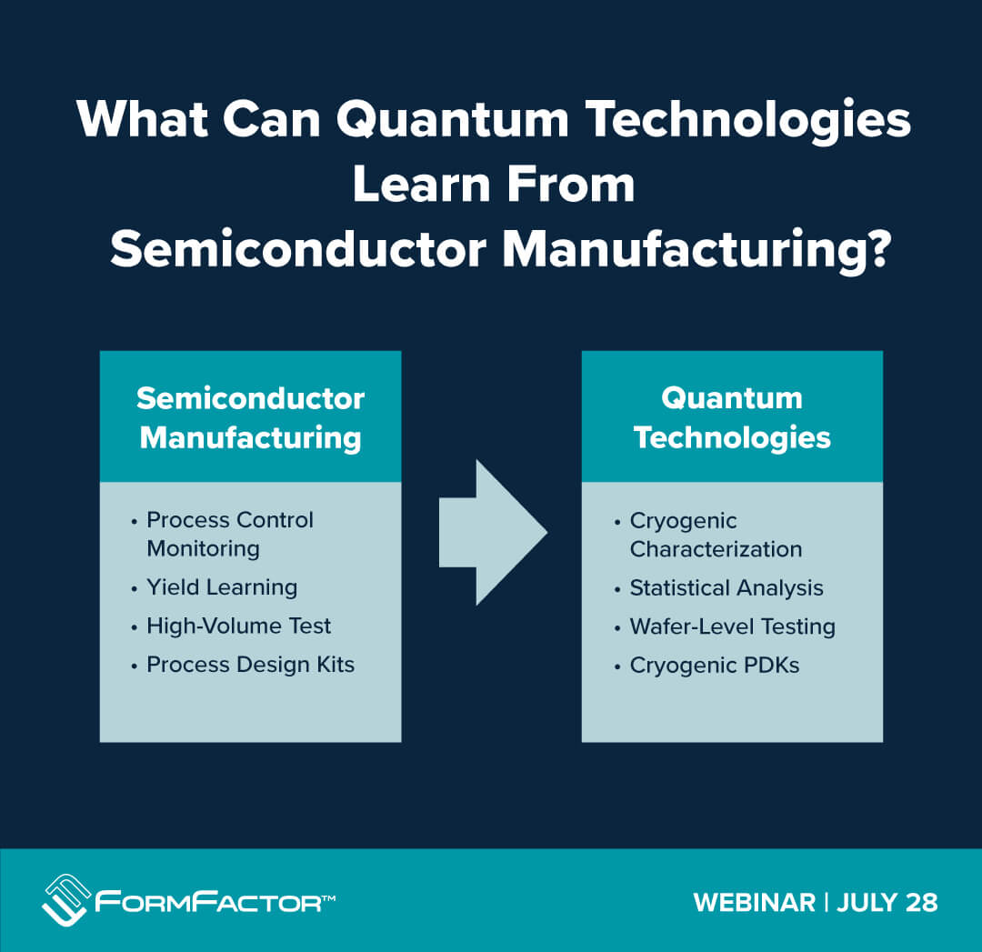
For more than 60 years, the semiconductor industry has shown how complex technologies can scale from early innovation to high-volume production. That progress was not driven by fabrication alone. It came from a repeatable framework built around process control, wafer-level test, yield learning, and close feedback between design and manufacturing.
Quantum computing, quantum sensing, and cryogenic electronics have made tremendous progress over the past decade. Now the industry is facing a different challenge. It is no longer just about proving these technologies work. It is about figuring out how to manufacture them reliably and at scale.
At the recent QED-C conference, Beverly Boiko, Sr. Principal Applications Engineer at FormFactor, explored how proven semiconductor manufacturing practices can help move quantum technologies closer to commercial production. Her presentation, Leveraging Semiconductor Fabrication Processes and High-Volume Test to Advance Quantum Technologies, outlined how wafer-level test, cryogenic characterization, and data-driven process learning can support the next phase of quantum development.
Quantum Is Entering Its Manufacturing Era
The semiconductor industry did not become successful because engineers built a few exceptional chips. It became successful because manufacturers learned how to build billions of devices with consistency, reliability, and predictable performance.
That same mindset is becoming increasingly important for quantum.
Whether engineers are building superconducting qubits, quantum sensors, cryogenic CMOS, or advanced readout electronics, they are running into many of the same manufacturing challenges the semiconductor industry solved years ago.
These challenges include:
- Process variability
- Device-to-device consistency
- Statistical characterization
- Manufacturing yield
- Scalable test methodologies
- Design optimization using production data
The good news is that semiconductor manufacturing already offers a well-established playbook for solving many of these problems.
Semiconductor Manufacturing Was Built Around Repeatability
Modern semiconductor fabrication depends on extraordinary process control. A single wafer may move through 80 to 120 fabrication loops, with repeated steps such as deposition, lithography, etching, cleaning, doping, and metrology.
At a high level, the manufacturing flow includes front-end wafer fabrication, wafer probe and electrical test, assembly and packaging, and system-level integration.
Every step in the process produces data that engineers use to improve manufacturing. Over time, those insights help reduce variation, increase yield, and make production more predictable.
This level of control did not happen overnight. It took decades of process refinement, testing, and data analysis to build the manufacturing systems the semiconductor industry relies on today.
Why Wafer Test Is Central to Manufacturing Success
It is easy to think of wafer test as the final inspection before packaging. In reality, it is one of the most valuable sources of manufacturing data.
Testing devices before packaging helps manufacturers identify process issues early, isolate sources of variation, and avoid adding cost to defective components. More importantly, wafer test creates the feedback loop that continuously improves manufacturing.
As production volumes increase, engineers can compare measured performance against design targets, identify systematic deviations, and make process corrections before defects become widespread.
This continuous feedback process, known as the yield learning cycle, has helped the semiconductor industry steadily improve manufacturing performance over decades.
For quantum technologies, that same type of feedback will be essential.
Process Control Monitoring Keeps Manufacturing on Track
Process Control Monitoring, or PCM, is a foundational part of semiconductor manufacturing.
PCM uses dedicated test structures built into production wafers to evaluate the health of fabrication processes. Instead of discovering problems after devices have been packaged, engineers can spot subtle process changes much earlier and correct them before they affect production.
Typical PCM structures can help monitor:
- Contact resistance
- Open and short circuits
- Via integrity
- Oxide quality
- Transistor performance
These measurements give process engineers the data they need to detect drift, identify root causes, validate process improvements, and maintain tighter control over manufacturing.
For quantum devices, this type of process visibility can be especially valuable because small fabrication changes can have a significant impact on device behavior.
Design Gets Smarter with Process Design Kits
Another reason semiconductor manufacturing scales so effectively is the use of Process Design Kits, or PDKs.
PDKs connect design intent to manufacturing reality. They provide engineers with device models, design rules, simulation data, and process constraints that help predict how a device will behave before it is fabricated.
As production data accumulates, PDKs become more accurate. That reduces design risk, shortens development cycles, and helps engineers build devices that are more likely to perform as expected.
There is every reason to believe the same approach can help accelerate quantum device development as well.
Quantum Devices Present New Test Challenges
Although many semiconductor manufacturing techniques translate well to quantum devices, testing at cryogenic temperatures introduces an entirely new set of challenges.
Many critical quantum device properties only appear at low temperatures. Superconductivity, certain material loss mechanisms, qubit behavior, and cryogenic transport effects cannot be fully understood through room-temperature measurements alone.
Measuring devices only at room temperature does not tell the whole story.
Small variations in fabrication can shift qubit frequency, affect resonator performance, increase loss, or reduce device stability. Without scalable cryogenic measurement data, these effects are difficult to quantify and even harder to control.
Bringing Wafer-Level Test into Cryogenic Environments
That is where cryogenic wafer probing becomes especially valuable.
Instead of evaluating a small number of packaged devices, engineers can characterize entire wafers under cryogenic conditions. This creates much larger datasets and gives teams a clearer view of how fabrication variation affects device performance.
Cryogenic wafer-level test can help engineers:
- Measure complete wafers under low-temperature conditions
- Compare room-temperature and cryogenic performance
- Identify process-induced variability earlier
- Improve feedback into fabrication
- Accelerate yield learning
Modern cryogenic wafer probing systems can also support automated wafer handling, wafer mapping, optical alignment, advanced probe cards, and software-driven test workflows.
Together, these capabilities make cryogenic testing far more practical for production environments, not just research labs.
The Next Step: Cryogenic PDKs
As engineers collect more cryogenic measurement data, the next logical step is building Process Design Kits specifically for low-temperature operation.
A cryogenic PDK would extend traditional semiconductor modeling to include low-temperature effects and quantum-relevant device behavior. These models may include:
- Superconducting material properties
- Junction behavior and variability
- Thermal conductivity
- Carrier freeze-out effects
- Cryogenic transport behavior
- Device-level statistical variation
Traditional PDKs changed how integrated circuits are designed. Cryogenic PDKs could have a similar impact on the future of quantum devices.
With better cryogenic models, engineers can make more informed design decisions before fabrication, reduce iteration cycles, and improve the connection between design, process, and test.
Scaling Quantum Requires a Manufacturing Mindset
Breakthroughs in quantum hardware will continue to push the industry forward, but commercial success will depend on much more than better devices. Manufacturers also need repeatable fabrication processes, scalable wafer test, and the ability to learn from production data.
That is where decades of semiconductor manufacturing experience become incredibly valuable. Practices like process control monitoring, yield learning, wafer-level characterization, and data-driven design have already transformed one industry. Applying those same principles to quantum technologies can help shorten development cycles, improve yield, and make commercial-scale production far more achievable.
As quantum technologies continue to mature, semiconductor manufacturing will not simply support the industry. It will help define how quickly it scales.
Learn More
For a deeper look at the methodologies, measurement approaches, and cryogenic test innovations discussed here, view the full presentation:
Leveraging Semiconductor Fabrication Processes and High-Volume Test to Advance Quantum Technologies