August 12, 2026
Comprehensive wafer-level characterization allows manufacturers to identify defects before packaging, optimize process performance earlier in development, and collect the measurement data needed to improve yields over time.
August 12, 2026
Comprehensive wafer-level characterization allows manufacturers to identify defects before packaging, optimize process performance earlier in development, and collect the measurement data needed to improve yields over time.
Artificial intelligence is reshaping the semiconductor industry at an unprecedented pace. As AI models grow larger and more complex, the infrastructure supporting them must move enormous amounts of data between processors, accelerators, memory, and storage with minimal latency and maximum efficiency.
That’s one reason silicon photonics (SiPh) has become one of the industry’s fastest-growing technologies. By replacing traditional electrical connections with optical communication, photonic integrated circuits (PICs) enable the high-bandwidth, low-power interconnects needed for 1.6T optical modules today and even faster 3.2T architectures in the future.
Designing these devices is only part of the equation. Before they can be deployed in next-generation AI systems, engineers need to verify that they perform exactly as intended. As device complexity increases, photonic integrated circuit testing has become one of the most demanding areas of semiconductor measurement and characterization.
Why Photonic Integrated Circuit Testing Is Different
Unlike conventional semiconductor devices, photonic integrated circuits combine electrical and optical functionality on the same chip.
A single PIC may integrate:
Since signals move back and forth between electrical and optical domains, engineers have to validate both at the same time. Success depends on measuring RF performance while maintaining precise optical alignment throughout the test process.
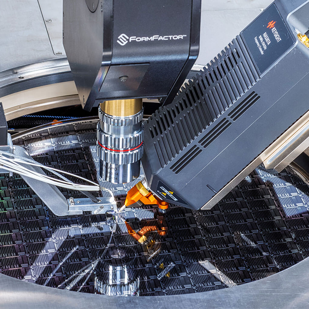
As silicon photonics moves from R&D into high-volume manufacturing, production-ready platforms like TRITON™ help automate wafer-level electro-optical testing while improving throughput and repeatability. Identifying performance issues early helps manufacturers:
That creates a testing environment unlike most traditional semiconductor applications, where RF engineering, optics, precision mechanics, automation, and motion control all have to work together seamlessly.
Challenge #1: Characterizing Devices Beyond 200 GHz
Bandwidth expectations continue to rise as the industry transitions toward 224 Gbps signaling and begins planning for 448 Gbps PAM4 systems.
At these data rates, engineers are no longer concerned only with the fundamental frequency. Harmonics increasingly affect signal integrity, device modeling, and overall system behavior.
Measurements that once peaked below 70 GHz are now extending beyond 130 GHz, with many advanced applications requiring characterization approaching 200 GHz and beyond.
To keep pace, engineers are adopting new measurement approaches that include:
The goal isn’t just to measure higher frequencies. It’s capturing reliable broadband performance in a measurement environment engineers can repeat with confidence.
Challenge #2: Achieving Repeatable Measurements
As frequencies climb, even the smallest errors become much harder to ignore.
At 220 GHz and above, even slight differences in probe placement or contact quality can influence measurement results. Variables that once had minimal impact become significant contributors to uncertainty, including:
Accurate measurements only matter if engineers can reproduce them every time. Repeatability is now just as important as bandwidth. Without consistent data, it’s difficult to build accurate device models or make confident design decisions.
This is why automated and semi-automated wafer probe systems are becoming standard tools in advanced RF and photonics labs. By reducing operator variability and controlling touchdown conditions more precisely, automation improves consistency across wafers, operators, and measurement sessions.
Challenge #3: Advanced Calibration for High-Speed Differential Measurements
As measurement bandwidth expands, calibration becomes an increasingly important part of the overall test strategy.
Many modern photonic integrated circuits use high-speed differential interfaces that introduce additional sources of measurement uncertainty. Crosstalk between adjacent probe structures and neighboring signal paths can distort results at frequencies where those effects were previously insignificant.
To maintain accuracy, engineers are adopting more sophisticated calibration techniques such as:
These approaches compensate for complex interactions within the measurement system and provide greater confidence across wide frequency ranges.
Today, calibration is much more than a final correction step. It’s a core part of producing accurate, trustworthy high-speed measurements.
Challenge #4: Maintaining Sub-Micron Optical Alignment
RF measurements are challenging on their own, but optical testing introduces a completely different set of obstacles.
Many wafer-level photonic tests require aligning an optical fiber with microscopic structures on the device under test. Depending on the application, the fiber may inject laser light into the device or capture light emitted from it.
Alignment tolerances are often measured in microns, and even tiny positioning errors can significantly affect measurement accuracy.
The task becomes even more difficult when the optical interface isn’t directly visible. Many photonic devices rely on trenches, V-grooves, or edge-coupling structures that limit visibility during testing, requiring engineers to position fragile optical fibers within extremely confined spaces.
To improve repeatability, today’s optical probing solutions increasingly incorporate:
Working together, these technologies help engineers achieve repeatable sub-micron alignment while reducing setup time and improving measurement consistency.
Why Wafer-Level Photonic Testing Matters
As photonic integrated circuits continue to evolve, testing is becoming a key differentiator, not just another manufacturing step.
Comprehensive wafer-level characterization allows manufacturers to identify defects before packaging, optimize process performance earlier in development, and collect the measurement data needed to improve yields over time.
The challenge is bringing multiple disciplines together into a single workflow. Successful photonic testing requires expertise in:
Success depends on bringing all of these capabilities together in one workflow, giving engineers the confidence they need from early device development through high-volume manufacturing.
Looking Ahead
As AI, high-performance computing, and hyperscale data centers continue to expand, demand for faster optical interconnects will only grow.
As photonic integrated circuits become more capable, the job of testing them becomes even more demanding. Higher frequencies, tighter alignment tolerances, more sophisticated device architectures, and increasing production volumes will all require continued advances in measurement technology.
Breakthroughs in photonic device design will certainly drive the next generation of AI infrastructure, but they’ll only reach production if engineers can measure and validate them with confidence.
As photonic devices become more complex, the ability to test them accurately and repeatably will play an increasingly important role in bringing the next generation of AI technologies to market.
FAQs – Photonic Integrated Circuit Testing
What is photonic integrated circuit testing?
Photonic integrated circuit (PIC) testing verifies the electrical and optical performance of semiconductor devices that integrate components such as lasers, modulators, photodetectors, and waveguides onto a single chip. Testing helps ensure devices meet performance specifications before packaging and production.
Why is wafer-level testing important for photonic devices?
Wafer-level testing allows manufacturers to identify defective dies before expensive packaging and assembly. This improves yield, lowers manufacturing costs, speeds process development, and ensures only known-good devices move to the next production stage.
Why are measurements above 200 GHz becoming necessary?
Emerging 224 Gbps and future 448 Gbps interconnects require broader bandwidth characterization than previous generations. Engineers must capture both fundamental signals and harmonic behavior to accurately evaluate device performance and signal integrity.
Why is optical alignment so difficult during PIC testing?
Many photonic devices require optical fibers to align with microscopic features using sub-micron precision. Limited visibility, fragile fibers, and complex coupling structures make accurate and repeatable alignment one of the biggest challenges in photonic characterization.