Moving Silicon Photonics from the Lab to the Fab
The semiconductor industry is at the gateway of a technology shift in the form of silicon photonics (SiPh), which holds the potential for spectacular gains in speed, power efficiency and density.
The first wave of the SiPh revolution stands poised to roll over data centers around the world with optical interconnects that breach the barriers set by copper wire. End user benefits might include an HD movie or 100 hours of music downloaded in a single second. Bandwidths of a terabit per second now come within practical reach.
FormFactor is already playing a significant role in the implementation of silicon photonics technology. This major inflection point provides a good illustration of how we participate in solving the challenges of wafer test long before a new technology goes into mass production.
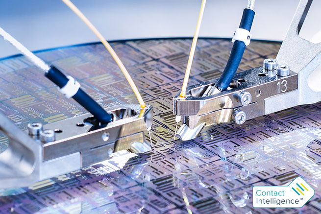
When optical fibers must be precisely aligned to couple light in and out of a wafer without physical contact
SiPh permits both logical and optical components to coexist on the same wafer. Optical devices such as lasers, waveguide structures, detectors, multiplexers and others could interface directly with classic logic components or can be combined as separate ICs through advanced 2.5D and 3D integration techniques. This new level of integration permits the fabrication of hybrid devices that can be mass produced and interconnected via optical fiber cabling at very low cost while yielding substantial performance gains.
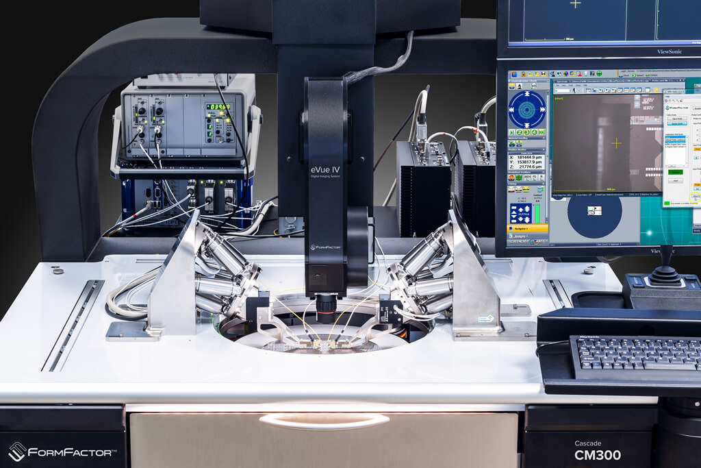
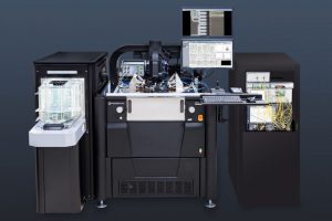
Automated Photonics Probing
Sophisticated optical alignment algorithms combine with high speed, high precision piezo control to optimize placement of input and output optical probes as the test sequence advances from one set of waveguides to the next and onto the next device.
Moving to a New Paradigm in Wafer Test
Typically, SiPh includes on-chip I/O devices in the form of etched diffraction gratings, which route the light from off-chip optical fibers to waveguides within the chip, where operations such as filtering and conversion to digital data streams are performed.
This addition of optical I/O, along with electrical, adds an entirely new dimension to wafer test methodologies. The need to capture and insert modulated beams of light requires the development of novel probing strategies that accommodate a new set of mechanical requirements. The classic problem of maintaining accurate physical probe contact with pads on the wafer surface gives way to a new paradigm when optical fibers must be precisely aligned to couple light in and out of a wafer without physical contact.
FormFactor understands the critical importance of refining and perfecting SiPh probe technology. The research at this phase of development will ultimately provide the foundation for wafer-level production test. And as SiPh technologies expand beyond the data center into a growing number of new applications, the costs associated with testing millions of devices will become a critical factor in realizing the full economic potential of SiPh.

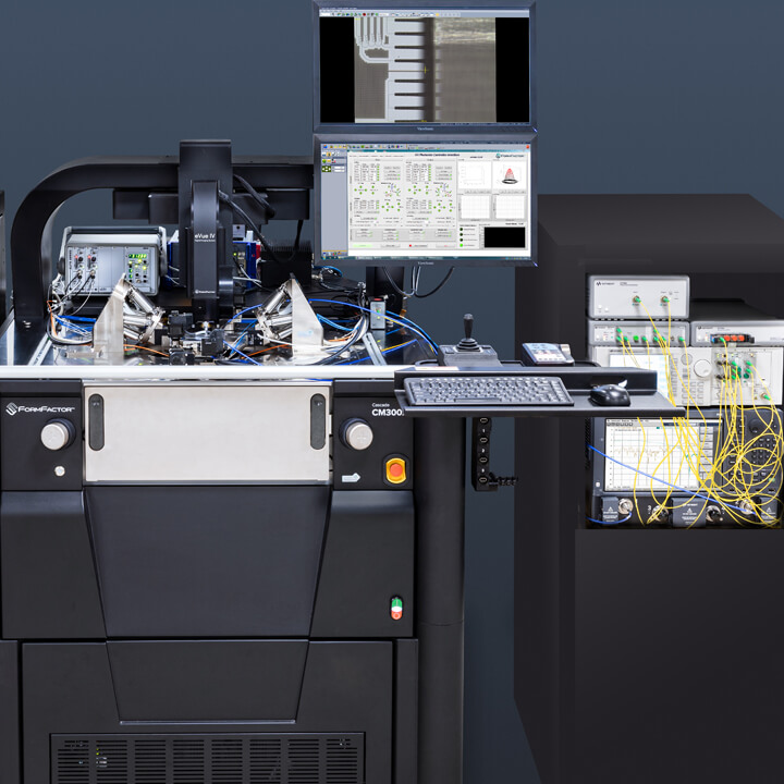
Alliances Hold the Key to SiPh Test Solutions
FormFactor takes a holistic view toward developing successful approaches to SiPh wafer test devices. We have forged partnerships with other key suppliers of test technology that play on each contributor’s individual strengths. In this particular application, we work with Preferred Partners Keysight Technologies for measurement instrumentation and Physik Instrumente (PI) for positioning technology. FormFactor leverages considerable expertise through an innovative team as well as collaborating with the right partners to deliver effective solutions.
Verified integrated Silicon Photonics 200mm and 300mm wafer probing solution for production-proven, optimized optical measurements right after installation.
SiPh-Tools is Key to the Integrated Solution

FormFactor’s SiPh-Tools is a powerful software package that includes a vast tool set for enabling and facilitating optical probing. By integrating probe station machine vision capability with optical positioning and even test equipment, SiPh-Tools automates manual tasks.
FormFactor Photonics Controller Interface (PCI)
FormFactor has developed the Photonics Controller Interface (PCI) application which provides a graphical user interface that allows flexibility for the user to manually control the optical positioning system. This feature-rich interface can also be used to setup scan parameter configurations and perform initial optical alignment functions among many other functions. Once aligned, all calibration functions are automated and performed through SiPh-Tools.

Horizontal Die-Level Edge Coupling

The best coupling efficiency for high bandwidth applications is achieved by getting fibers/arrays as close as possible to the exposed waveguide facet(s) through horizontal die-level edge coupling. True edge coupling enables close simulation of real-world conditions with device performance closest to the final application.
FormFactor provides the only solution on the market that enables advanced automated alignment for horizontal die-level edge coupling, deploying exclusive automated fiber-to-facet alignment techniques and reducing the risk of damaging fibers to a minimum with collision avoidance technology.
Unique software algorithms like AlignOpticalProbes3D enable optimizing the fiber-to-facet gap versus maximum coupled power at both the input and output simultaneously.
No other solution available enables you to get the positioning hardware calibrated in the YZ plane and ready to perform edge coupled optical optimizations.
Wafer-Level Edge Coupling
Wafer-level edge coupling is now possible with a new innovative combination of hardware and software features to align and optimize fibers/arrays in a wafer-level trench.
A suite of software alignment algorithms enable YZ optimization scans in a wafer trench while tapered lensed fiber holders provide a low approach angle relative to the wafer surface. This enables alignment of the probe in the trench as close as possible to the facets, minimizing coupling losses with minimal trench dimensions.
The solution means easy setup even for less experienced users, repeatable measurement results due to unique fiber-to-facet gap alignment technology, and reduced risk of damaging fibers with collision avoidance technology.

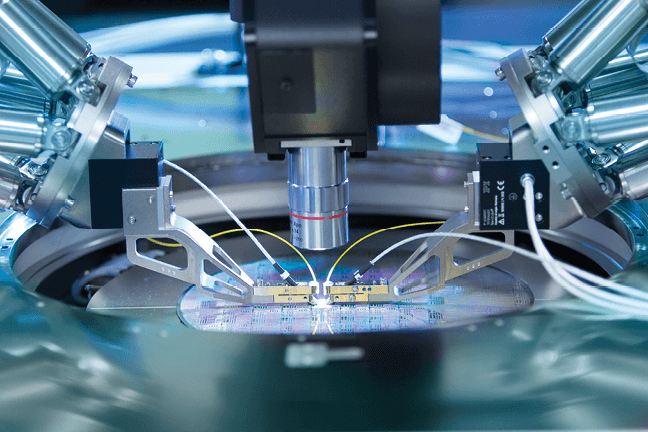
Vertical Coupling

FormFactor’s technology has become the industry standard for vertical coupling to wafer-level grating couplers. No other solution available gets the positioning hardware calibrated to the probe station and ready to perform die-to-die optical optimizations in minutes. With exclusive calibrations like Pivot Point, the optimal point of minimal translation at the fiber/array tip is automatically determined. Using this Pivot Point, FormFactor’s Incident Angle Optimization routine enables you to determine best position to maximize coupling efficiency. Knowing how the optimized incident angle compares to designed incident angle can lead to discovery of fab or other process defects.
OptoVue and OptoVue Pro

FormFactor brings a revolutionary technology advancement for wafer and die-level photonics probing with its OptoVue and OptoVue Pro. This feature includes advanced calibration technologies with more viewing directions and significant additional features that enable faster time to more accurate measurement results.
Situated in an auxiliary chuck location on the CM300xi, OptoVue and OptoVue Pro enable calibrations to be performed in-situ without removing the test wafer to put a calibration wafer on the chuck. This CalVue feature enables seamless calibrations without operator interaction, resulting in faster time to measurement and reduced cost of test.
OptoVue Pro includes a feature-rich set of tools for optical probing including DieVue for die-level probing of singulated photonic devices, ProbeVue for inspecting and measuring fibers and fiber arrays, and PowerVue for measuring laser power at the probe tip.