Generative AI is changing what semiconductor systems need from memory. As AI models grow, inference workloads become more demanding, and enormous volumes of data move between compute and memory, system performance increasingly depends on how quickly and efficiently that data can be accessed.
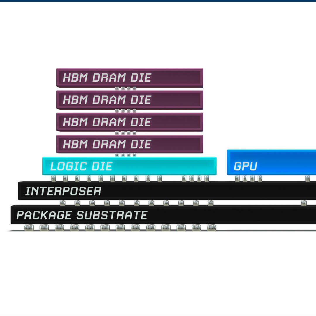
High Bandwidth Memory (HBM) has become a critical part of that equation. But the HBM roadmap is no longer simply about adding more bandwidth. New architectures are bringing memory and logic closer together through advanced logic base die, custom PHYs, workload-optimized memory controllers, and increasingly application-specific functionality.
For semiconductor test engineers, these changes create a new set of challenges. Higher I/O density, taller stacks, faster interfaces, greater power requirements, and more complex logic all need to be tested reliably at wafer level and under increasingly demanding conditions.
In FormFactor’s upcoming webinar, Enabling GenAI Through Advanced MEMS Probe Card: Scaling HBM and Custom HBM Test for High-Temperature, Fine-Pitch, and μBump-Array Pad Applications, our experts will explore what these changes mean for HBM test and the probe card technologies needed to keep pace.
HBM Is Scaling Faster Than Ever
HBM has already helped address one of the fundamental challenges facing AI computing: keeping increasingly powerful processors supplied with data. But HBM is quickly becoming more than a way to feed data to increasingly powerful processors.
Industry roadmaps point to continued progression from HBM3E toward HBM5, accompanied by major increases in stack height, I/O density, bandwidth, and logic integration. I/O counts are expected to scale from approximately 1,024 toward 4,096, while future devices move toward 16-Hi and potentially 20-Hi stacks.
At the same time, the architecture itself is changing. Earlier HBM implementations used base dies manufactured in a DRAM process and standard DDR PHYs. Emerging HBM and Custom HBM designs are introducing custom PHYs, workload-optimized controllers, and more advanced logic within the base die. That gives semiconductor companies more freedom to optimize memory architectures around specific workloads, including AI training and inference.
Memory, logic, and compute are becoming much more tightly integrated, giving designers more options to optimize HBM for specific AI workloads. That can deliver significant system-level benefits, but it also changes what needs to happen during test.
Why HBM Test Is Becoming More Challenging
As HBM stacks get taller, hotter, faster, and more densely interconnected, adding more probes is only part of the test challenge.
Thermal behavior is one example. As additional dies are added to the stack, thermal resistance can increase, driving higher operating temperatures across the core and base dies. Test hardware must continue to deliver reliable electrical contact even as the device and test environment experience significant thermal changes.
For the probe card, that means maintaining planarity, stable contact resistance, and consistent scrub performance across the test area. Those requirements become harder as temperatures increase and different materials expand at different rates.
Higher interface speeds make the test problem even more difficult. Custom PHY architectures are being developed to increase performance while making more efficient use of die area. As interface speeds rise, probe cards must support the high-frequency performance required to validate increasingly advanced HBM and Custom HBM interfaces. High-frequency signal integrity is becoming an increasingly important requirement as interface speeds continue to scale.
Physical complexity is increasing as well. More logic in the base die, increasingly sophisticated controllers, finer pitches, and dense μBump-array pad structures can dramatically increase the number of electrical connections required during test.
Next-generation HBM probe card requirements can include:
- High-speed testing at frequencies exceeding 5 GHz
- Chuck temperatures above 125°C
- Increasing current-carrying requirements
- Reliable contact across dense, fine-pitch pad arrays
- More than 80,000 probes per device under test (DUT)
The real challenge is meeting all of these requirements at the same time without sacrificing measurement accuracy or repeatability.
The Probe Card Has to Evolve with HBM
For advanced HBM, simply making reliable electrical contact is no longer enough. The probe card must maintain consistent mechanical behavior across a large and densely populated test area while accommodating thermal expansion. It must provide stable electrical performance as frequencies and current requirements rise. And it must repeatedly contact increasingly complex pad structures while maintaining contact uniformity, stable contact resistance, and precise alignment across dense test areas.
That puts probe card performance squarely in the middle of the HBM test strategy.
Advanced MEMS architectures offer several advantages for these applications because they can combine high probe density with tightly controlled mechanical and electrical characteristics. FormFactor technologies such as SmartMatrix™ and MEMS vertical probe cards are designed to address the thermal, electrical, mechanical, and density requirements associated with advanced HBM and Custom HBM testing.
The need for that flexibility grows as more logic moves into HBM architectures. Test requirements begin to cross traditional boundaries between memory and logic test, requiring probe technologies that can support a broader range of device architectures and operating conditions.
Upcoming Webinar: Enabling GenAI Through Advanced MEMS Probe Card Technology
FormFactor’s upcoming webinar, Enabling GenAI Through Advanced MEMS Probe Card: Scaling HBM and Custom HBM Test for High-Temperature, Fine-Pitch, and μBump-Array Pad Applications, takes a closer look at these challenges and the technologies being developed to address them.
Attendees will learn about:
- Compute and memory trends driving next-generation HBM and Custom HBM
- How increasing stack height affects thermal behavior and test requirements
- High-speed HBM testing at frequencies exceeding 5 GHz
- Testing at chuck temperatures above 125°C
- Managing signal integrity, contact resistance stability, probe planarity, and thermal expansion
- Establishing reliable contact across dense μBump-array pad structures
- Probe architectures supporting more than 80,000 probes per DUT
- How advanced MEMS probe card technology can address emerging HBM test requirements
This webinar is the first installment in a new series exploring how semiconductor test technologies are helping enable the silicon innovations behind the GenAI era.
Register for the session that works best for your region:
Join FormFactor to learn how advanced MEMS probe card technologies are helping engineers tackle the thermal, electrical, mechanical, and density challenges that come with next-generation HBM and Custom HBM devices.