April 8, 2026
Modern semiconductor probe stations must deliver sub-micron positioning accuracy, ultra-low noise measurement integrity, wide thermal control ranges, and high-frequency stability, all while supporting increasing automation demands.
April 8, 2026
Modern semiconductor probe stations must deliver sub-micron positioning accuracy, ultra-low noise measurement integrity, wide thermal control ranges, and high-frequency stability, all while supporting increasing automation demands.
As semiconductor devices scale to advanced nodes and heterogeneous architectures, the probe station (or probe system as they are sometimes called) has become far more than a lab instrument. It is now a critical enabler of wafer-level test, yield optimization, and performance validation for AI processors, 5G RF devices, chiplets, and advanced packaging technologies.
Modern semiconductor probe stations must deliver sub-micron positioning accuracy, ultra-low noise measurement integrity, wide thermal control ranges, and high-frequency stability, all while supporting increasing automation demands. For engineering teams working at the leading edge, the probe station is no longer optional infrastructure. It is foundational to device performance and manufacturing success.
Wafer testing (also known as wafer sort) verifies device functionality prior to dicing and packaging, preventing downstream yield loss and cost escalation. As complexity rises, so does the importance of precise, repeatable on-wafer measurement.
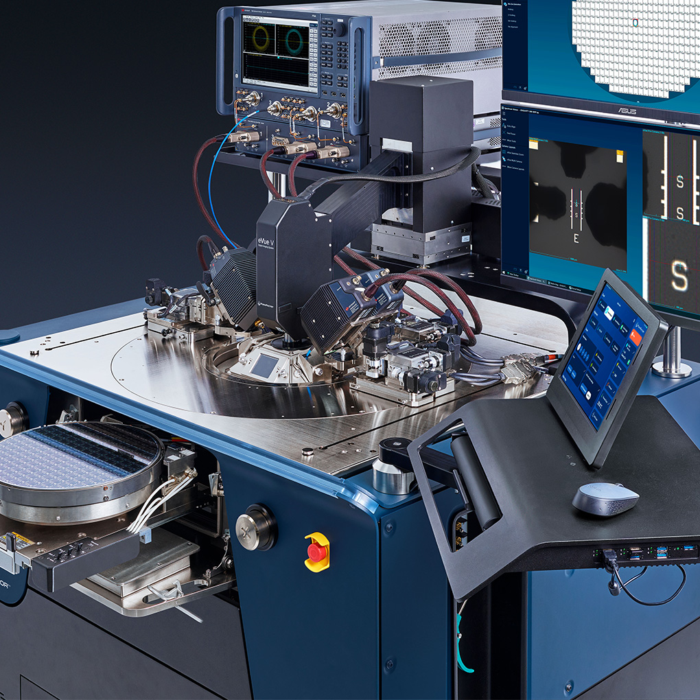
FormFactor’s portfolio of probe systems supports research, device characterization, and production wafer test across these advanced applications. Today’s environments span cryogenic probe stations, microwave probe stations, automated probe stations, and high-precision semiconductor probe stations, reflecting just how demanding modern test challenges have become
AI and High-Performance Compute Demand Extreme Parametric Precision
Wafer-level testing for AI processors push process nodes into single-digit nanometer regimes, where parametric margins are razor thin and power density is extreme.
In these devices:
That means probe stations must deliver:
Even small measurement instability at wafer test can translate into incorrect binning decisions or masked reliability risks.
FormFactor highlights the critical role of wafer-level test in AI devices in its video, The Vital Role of Semiconductor Wafer Test in Artificial Intelligence Devices.
For production flows, automated wafer-level parametric testing improves repeatability and reduces operator-induced variability.
Automation isn’t just about testing more wafers per hour, it’s about ensuring every data point reflects true device behavior, not environmental or mechanical instability.
5G and mm-Wave Push RF Probe Stations to Their Limits
5G infrastructure, phased-array modules, and emerging 6G research rely on high-frequency RF characterization at wafer level. Devices operating in mm-Wave bands introduce entirely new signal integrity challenges.
At these frequencies:
Even the slightest vibration or temperature shift can throw off your data.
High-performance microwave probe stations must address:
FormFactor’s RF-capable probe systems are designed to maintain signal integrity in demanding high-frequency environments.
As RF validation shifts earlier into wafer test to reduce packaging waste, engineering teams increasingly rely on probe stations that combine high-frequency accuracy with automation and environmental control.
Cryogenic Probe Stations Enable Quantum and Advanced Physics Breakthroughs
Quantum computing, superconducting electronics, and advanced materials research operate at cryogenic temperatures where traditional test platforms simply cannot function.
A cryogenic probe station must maintain electrical integrity and mechanical precision while operating across wide temperature ranges, from 300K down to liquid nitrogen temperatures and beyond.
In these environments:
This marks a major shift in probe station design, where controlling the environment is just as critical as measuring the device itself.
FormFactor supports cryogenic measurement platforms that provide stable temperature control and measurement reliability across wide ranges.
As quantum technologies transition from lab research to scalable platforms, cryogenic probe stations must minimize cooldown cycles, reduce drift between thermal states, and maintain calibration integrity across multiple measurement sessions.
Advanced Packaging and Chiplets Increase Mechanical and Electrical Complexity
The rise of chiplet architectures and 2.5D/3D integration has dramatically increased the importance of wafer probe testing prior to stacking and bonding.
In advanced packaging flows:
Known Good Die (KGD) validation at wafer level is essential. Optimized wafer testing techniques directly enhance semiconductor yield and reduce manufacturing risk
But advanced packaging also introduces new mechanical challenges:
In the chiplet era, mechanical precision and electrical performance have to work hand in hand.
Probe stations must support:
These capabilities directly impact final assembly yield and long-term reliability.
Software Integration Is Now a Performance Multiplier
Modern probe stations are not standalone tools, they are part of an integrated test ecosystem.
FormFactor’s probe station control software enhancements demonstrate how intelligent motion control and workflow automation improve measurement consistency.
Key capabilities include:
For engineering managers, this reduces training complexity, shortens debug cycles, and improves reproducibility across teams and facilities.
Automated vs. Manual Probe Stations: Strategic Tradeoffs
Manual probe stations remain valuable for:
They provide flexibility and lower initial cost.
However, automated probe stations deliver significant ROI in environments requiring:
Automation reduces operator variability and protects measurement integrity across large datasets
The decision ultimately depends on:
The Future of Probe Station Technology
AI pushes parametric precision to its limits. 5G and mm-Wave demand high-frequency stability. Quantum research redefines environmental control. Advanced packaging increases mechanical complexity.
Today’s probe station isn’t just a characterization tool, it’s a critical link in protecting yield, validating performance, and accelerating innovation across the semiconductor value chain.
Engineering teams evaluating their next platform should ask:
Thinking through these questions now can make the difference between keeping up, and leading, the next wave of semiconductor innovation.