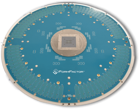
We recently announced the availability of our new Altius™ vertical MEMS probe card designed to address the wafer test challenges associated with 2.5/3D advanced packaging technologies.
Adoption of advanced packaging is accelerating thanks in part to the classic Moore’s Law and transistor shrink diminishes. Advanced packages enable the heterogenous integration of multiple different die through high-density interconnects, for improved device performance and smaller footprint. According to Yole Développement, the overall advanced packaging market will grow at an 8% CAGR, reaching almost US$44 billion in 2024.
Altius supports ultra-low force probing at 45 µm grid-array contact pitch, with a scalable roadmap for future IC package pitch reduction. It enables cost-effective wafer or die test of a variety of components in a heterogenous integrated system, from validating at-speed performance of high bandwidth memory (HBM), to ensuring the integrity of high-density interconnects such as silicon interposers and embedded bridges.
Some of the key benefits of the Altius probe card include:
- Minimum grid-array pitch of 45 µm
- Ultra-low probe force for direct probing on copper through silicon vias or solder microbumps, ~1 gram per probe at operating overtravel with best-in-class contact resistance stability
- Support for HBM known-good-die or known-good-stack test, >= 3 Gbps test speed
- Scalable for multi-site test to increase throughput, X4 capable for HBM
- Configurable with Hybrid MEMS probes for mixed-pitch microbump layout
These features help make the Altius probe card the choice for the world’s leading test floor manufacturing of the highest performing commercially available logic devices in the market today.