FormFactor stands as the singular test and measurement company offering solutions to assist customers in validating device performance and yield across all phases of system integration. Our probe cards aid customers in reducing overall manufacturing costs and empower them to acquire enhanced intelligence and insights at each stage of this evolving process. This, in turn, supports them in making pivotal decisions related to test strategies, spanning from the laboratory to the fabrication facility.
In the past, wafer-level testing in semiconductor device production was relatively straightforward, but advancements in technology have transformed this landscape. The demand for cost-effective performance in high-end applications, such as data centers, artificial intelligence, autonomous vehicles, and hyper-realistic graphics, has led to the integration of multiple dies into monolithic systems. This shift comes at a time when Moore’s Law alone cannot guarantee the price/performance advancements of the past.
To address these processing demands, innovative solutions have emerged in the form of advanced packaging technologies, allowing for scaling and performance gains independent of on-chip feature size. High Bandwidth Memory (HBM), employing 3D vertical stacking of DRAM memory, pushes graphics processing silicon to unprecedented levels. Fan Out Wafer Level Packaging (FOWLP), utilized by Apple and TMSC, offers power savings and smaller footprints in portable devices. On the horizon, Heterogeneous Integration (HI) technology, like Intel’s system-in-package (SiP), enables the integration of dies from different wafers onto a single system substrate with extremely high interconnect density.
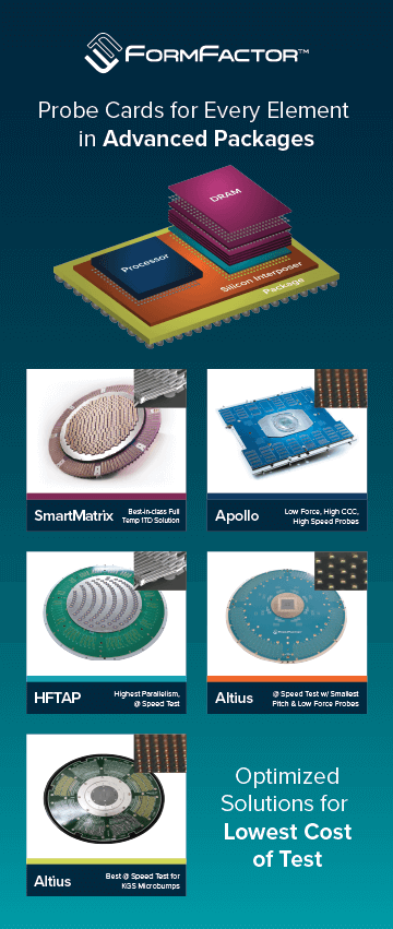
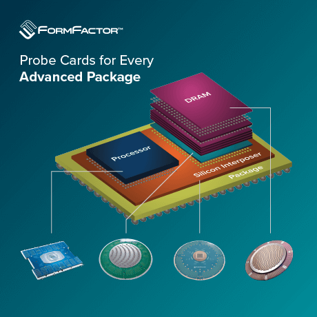
For these packaging paradigms to be cost-effective, they demand highly optimized and accurate fabrication processes. In a multi-die system, a single defect in a die or integration layer comes at a considerable cost. Consequently, wafer-level testing now spans multiple phases of the production process, positioning FormFactor as a key player in the development of advanced packaging technology. We have probe cards for every IC in advanced packaging, including:
SmartMatrix™ – Offers full-wafer contact testing on 300 mm wafers for mobile and commodity DRAM, graphic memory (GDDR), high bandwidth memory (HBM), and emerging memory devices. Tailored for swift design ramps and advanced product roadmaps, this platform expands the Matrix™ architecture, proven in production, to cater to heightened probe card parallelism, exceeding 3000 sites per wafer in a single touchdown.
Apollo – These vertical probe cards are well-suited for probing applications involving area-array and perimeter-layout, encompassing flip chip, pre-bump, or aluminum pad applications. Apollo stands out as the industry-preferred flip chip probe card for graphics processors, game console microprocessors, and automotive microcontrollers. Harnessing proprietary manufacturing technology, Apollo ensures exceptional reliability and quality for multi-DUT testing, with technological scalability to meet a diverse array of testing needs.
Altius™ – Crafted to address the demanding requirements of testing high-end logic and silicon interposer applications, the Altius probe card boasts a skate-shaped probe tip, a 45 μm pitch capability, low path resistance, and minimal leakage. It stands as the preferred choice for the world’s leading test floor manufacturing, catering to the production of the market’s highest-performing commercially available logic devices.
HFTAP Series – Utilizing an advanced MEMS probe card architecture, this system is employed to validate both the electrical performance and yield, not just for individual chips but also for the devices within the HBM stack. This includes the fine-pitch interposer, ensuring the comprehensive performance of the entire package.