As semiconductor devices scale to advanced nodes and higher levels of integration, wafer test has become one of the most critical steps in ensuring performance, yield, and long-term reliability. At the center of wafer-level testing is the probe card, a precision interface that connects automated test equipment (ATE) to devices under test on the wafer.
Probe card technology has evolved significantly over the last several decades. Traditional probe cards laid the foundation for semiconductor wafer testing, but increasing pin counts, tighter pitches, higher frequencies, and emerging applications such as AI accelerators and advanced memory have driven broader adoption of MEMS-based probe card architectures.
This guide provides a detailed comparison of MEMS probe cards and traditional probe cards, helping test engineers and decision-makers understand the trade-offs, performance differences, and selection criteria for modern wafer testing.
Evolution from Traditional Probe Cards to MEMS Technology
Traditional probe cards dominated early wafer testing due to their relatively simple construction and proven reliability. However, shrinking geometries and increasing I/O density exposed fundamental limitations in traditional designs.
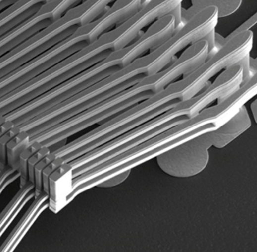
MEMS (Micro-Electro-Mechanical Systems) technology introduced a new approach, enabling probe structures fabricated using lithographic and microfabrication processes similar to semiconductor manufacturing. This shift allows significantly improved placement precision, scalability, and mechanical repeatability, which are key requirements for advanced wafer testing.
Traditional Probe Cards: Design, Capabilities, and Limitations
Traditional probe cards typically use cantilever or vertical needle probes made from tungsten or similar metals. These probes are mechanically assembled and aligned to contact wafer pads.
Key strengths of traditional probe cards include:
- Lower upfront cost for simpler applications
- Proven performance in mature process nodes
- Flexibility for lower pin-count designs
Limitations include:
- Reduced contact accuracy at fine pitches
- Variability introduced by manual assembly
- Limited scalability for high pin-count devices
- Increased maintenance as needles wear or deform
These constraints become more pronounced in advanced wafer test environments.
MEMS Probe Cards: Architecture, Materials, and Working Principles
MEMS probe cards use microfabricated probe elements built with precise lithographic processes. These probes are typically formed from silicon-based structures combined with conductive materials designed for durability and electrical performance.
Core advantages of MEMS probe card architecture:
- Sub-micron placement accuracy
- Highly uniform contact distribution across large probe arrays
- Excellent planarity and repeatability
- Compatibility with high-density and advanced-node devices
FormFactor’s MEMS technology is designed to meet the demands of leading-edge wafer test applications: https://www.formfactor.com/technologies/mems/
MEMS vs. Traditional Probe Cards: 10 Key Differences That Matter in Wafer Test
Below we compare MEMS probe cards and traditional probe cards across 10 factors that most directly impact wafer test performance, yield, and cost of ownership.
1. Contact Accuracy and Placement Precision
MEMS Probe Cards: Microfabricated structures deliver highly repeatable, sub-micron contact placement, critical for fine-pitch pads at advanced nodes.
Traditional Probe Cards: Mechanical assembly introduces variability that becomes limiting as pad sizes shrink.
2. Signal Integrity at High Frequencies
MEMS Probe Cards: Designed with controlled impedance and low parasitics, enabling reliable high-frequency wafer testing for RF, AI, and high-speed digital devices.
Traditional Probe Cards: More susceptible to signal loss and noise at higher frequencies.
3. Scalability for High Pin-Count Devices
MEMS Probe Cards: Scale efficiently to thousands of contacts, supporting dense I/O layouts used in advanced logic and SoCs.
Traditional Probe Cards: Scaling complexity and alignment challenges increase rapidly with pin count.
4. Contact Force Uniformity
MEMS Probe Cards: Highly uniform force distribution across all probes reduces pad damage and improves test repeatability.
Traditional Probe Cards: Force variation can lead to inconsistent contact resistance and higher retest rates.
5. Durability and Operational Lifetime
MEMS Probe Cards: Engineered for predictable wear and long lifetime in high-volume wafer test environments.
Traditional Probe Cards: Probes can deform or wear unevenly, increasing maintenance requirements.
6. Maintenance and Downtime
MEMS Probe Cards: Longer intervals between maintenance cycles help maximize tester uptime.
Traditional Probe Cards: Require more frequent cleaning, re-alignment, and refurbishment.
7. Performance at Advanced Nodes
MEMS Probe Cards: Well-suited for advanced-node devices where tight tolerances and repeatability are mandatory.
Traditional Probe Cards: Often better suited for mature nodes with larger geometries.
8. Impact on Wafer Test Yield
MEMS Probe Cards: Consistent contact quality reduces false fails and improves yield.
Traditional Probe Cards: Greater variability can negatively impact yield in demanding test conditions.
9. Test Throughput and Efficiency
MEMS Probe Cards: Improved signal quality and contact stability support faster test times and higher throughput.
Traditional Probe Cards: May require slower test speeds to maintain accuracy.
10. Total Cost of Ownership
MEMS Probe Cards: Higher upfront cost, but lower total cost of ownership through longer life, reduced maintenance, and yield gains.
Traditional Probe Cards: Lower initial cost, often suitable for less complex wafer test applications.
Consolidated Takeaways from the MEMS vs. Traditional Comparison
Across contact accuracy, signal integrity, scalability, durability, and maintenance, MEMS probe cards are optimized for advanced wafer testing where fine pitch, high pin count, and repeatability directly impact yield and throughput. Traditional probe cards continue to serve an important role in mature nodes and lower-complexity devices, where cost sensitivity and flexibility may outweigh the need for extreme precision.
For engineers evaluating probe card technologies, the decision is rarely based on a single parameter. It is the combined effect on tester uptime, wafer test yield, and long-term cost of ownership that ultimately determines the right solution.
Summary Comparison: MEMS vs. Traditional Probe Cards
MEMS probe cards represent a significant advancement in wafer probe card technology, delivering the precision, scalability, and electrical performance required for modern semiconductor testing. Traditional probe cards continue to play a role in less demanding applications, but MEMS technology is now the foundation for advanced wafer test strategies.
Choosing the right probe card technology is ultimately a balance of performance requirements, cost considerations, and long-term manufacturing goals. With deep expertise across both traditional and MEMS-based solutions, FormFactor helps engineers select the optimal probe card for every wafer test challenge.