The explosive growth of smart phones has driven advancements in communications protocols, such as 4G and 5G resulting in technological improvements in the backhaul infrastructure. The Internet of Things (IoT) is catching up in a big way which is leading newer applications for short-range communications and huge growth in Big Data. This increased demand, particularly among consumer applications, has shortened product life cycles, thus increasing the pace of RF technology development. To remain competitive, engineers must reduce cycle times and cost.
To address these issues, high-frequency probes (GHz and above) were developed and have significantly advanced on-wafer modeling and characterization capabilities. On-wafer probing at 40 GHz and beyond has developed from a simple R&D curiosity to a sophisticated high-volume tool used in device modeling, circuit development and manufacturing of RFIC’s, high-frequency packaging and hybrid technologies. The advancements made by Si-based technologies have also introduced the additional challenge of probing aluminum pads.
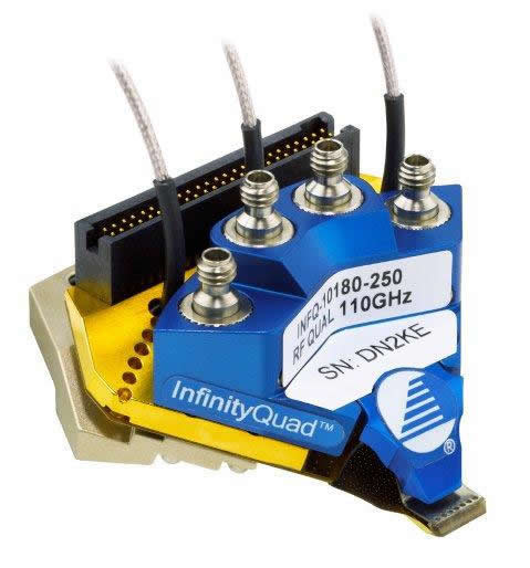
Our Infinity Probe technology has been designed to not only meet the challenges of high-frequency probing but also to meet the demands of stable contact resistance on aluminum pads. Successful high-frequency probing also requires that consideration be given to layout and design before design completion and mask fabrication. Failure to observe specific layout requirements can result in the inability to test devices with high-frequency probes.
It is useful to stop and consider what you really wish to measure. When high-frequency probes are used with a network analyzer (after calibration), what is measured will be what the probe tips contact. This includes the pad parasitics, and parasitics associated with the interconnects from the pad to the other devices on your substrate. If you want to measure a device independent of the pad effects, then it is useful to make the pads small, so their effects will be negligible or easily subtracted (de-embedded) from the measured data. In any event, it is important to be clear that when using a network analyzer you will be measuring everything past the end of the probe tips, unless you use special calibration/correction techniques. In most applications this is exactly what you want; a measurement of the circuit’s electrical performance.
 There are several physical features of Infinity probes that affect the mechanical layout. The first of these (see image to the right) is the extension of the probe tip substrate material and epoxy overcoat past the center of the contact closest to the edge.
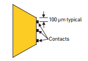
Another physical layout consideration is the probe contact size, typically 12 x 12 μm. Note that these contacts might be larger than needle probes, and the passivation windows must be large enough to accommodate these contacts plus typical probe system variations. This dimension is typically 100 μm. Probes must not be allowed to collide, so this 100 μm extension must be considered when laying out pads.
The final consideration is the probe skating distance. For every 50 μm of overtravel (overtravel is the continued downward movement after the probe tip has made initial contact with the wafer), the probe contacts will skate laterally 25 μm (2:1 overtravel to skate ratio). If the probes are too close together, they could skate into each other and be damaged. The layout rules will help you to prevent probe collisions.
Check out the Infinity Probe® Mechanical Layout Rules Application Note to discover how to successfully probe a fabricated device. In our next post, we’ll explore the sequence of layout events and what those layout rules are.