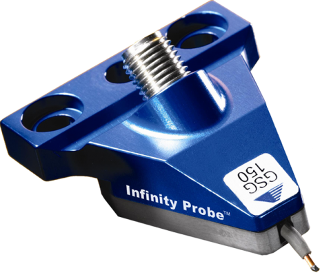
In a recent post, we discussed Infinity Probes and the features that affect mechanical layout. In this follow up post, we’ll review the sequence of layout events and what those layout rules are.
The following are guidelines for the typical sequence of events involved in layout for testing with Infinity Probes.
- Select basic pad footprint for ground-signal-ground (GSG), or signal-ground (SG) / ground-signal (GS), to be consistent with input/output type (see step 2), and if applicable, package requirements.
- Orient high-gain signal pads away from each other. Typical microwave devices place inputs on the left, and outputs on the right.
- The ground pads for each Infinity Probe must be electrically connected together on the input and output to provide a low-impedance common-ground node.
- Verify that pad pitch matches available probe pitch (see Probe Selection Guide). Also, verify that the pad footprint meets potential packaging requirements.
- If you must violate any of the layout rules, please contact Cascade Microtech regarding the trade-offs and to verify that the footprint is a good layout for probing. Some of the rules can be successfully violated, provided certain conditions are met.
Now let’s discuss the rules regarding probe pad placement and sizing. In many designs, the probe pads are also used as bond pads, so the final layout may need to satisfy requirements for both probing and bonding. A good layout for probing is usually also a good layout for packaging.
There are two important probe mechanical parameters, which directly affect the mechanical layout rules; the contact dimensions and the substrate extension past the contact. Typical contact size for Infinity Probes is 12 x 12 μm. The contact size is important because the passivation window must be large enough to allow the entire contact to touch the pad. The substrate extension is typically 100 μm past the contact center.
Infinity Probes are constructed with all contacts in a straight line, and with equal spacing between contacts. This means that all pads, arranged for an individual high-frequency probe measurement, must be in a straight line, have equal pitch, and be on top of the substrate. Non-square or very large pads may be laid out more randomly, as long as there is a minimum-size land area, spaced at an equal pitch for the probe contacts to land on.
All pads must have minimal height variation, because probe construction allows little contact height variation.
If the probes skate into each other, they can be damaged. The pad layout must allow for sufficient damage avoidance space between probes. Provide sufficient space for probes that are oriented 90 degrees to each other, as well as between probes that face each other. There must be sufficient space between probes to allow for probe skating. The following pad layout rules allow for vertical overtravel of 6 mils (152.4 μm). Note that 6 mils is the maximum suggested overtravel for Infinity probes, and that the recommended nominal overtravel (to achieve assured contact) for the typical probe is 2-3 mils (50-75 μm).
- The minimum pad size for manual probe placement is 25 x 35 μm. (Note the longer dimension on the rectangular pad is in the direction of probe skate.) The recommended minimum pad size for general use (auto or semi-auto probe placement) is 50 x 50 μm. For narrow pitch probes (e.g. 50 or 75 μm pitch) minimum pad size is 30 x 50 μm. Unless you have a good reason to do otherwise, use 100 x 100 μm pads with a 150 μm pitch. This provides for easy probing, and parasitics are low enough for many applications.
- The minimum passivation window size is 25 μm x 44 μm. Note that for small pad sizes, the passivation window will be larger than the pad. However, because of reliability considerations, it’s not considered good practice to have the passivation window larger than the probe pad. If the pad metallization is above the final passivation layer, this rule does not apply. To provide clearance for the probe tip, the distance from the top of the probe pad to the top of passivation layer should not exceed 40 μm. Lastly, the passivation window must allow the probe tips to come to rest in their measurement position of 25 μm from the leading-edge of the probe pad. This position corresponds to the same pad overlap that is used during calibration.
- The minimum center-to-center pad pitch is 50 μm. 150 μm is recommended.
- The minimum center-to-center pad spacing for orthogonally oriented probes (in a corner) is 200 μm. Sufficient clearance is often achieved by eliminating the corner pad.
- The minimum center-to-center pad spacing for opposing, side-by-side probes that are contacting the same line of pads, is 200 μm.
- The minimum center-to-center pad spacing between facing probes on parallel rows of pads is 150 μm. Note that this spacing is based on the assumption that no more than 6 mils (150 μm) of probe overtravel (maximum allowed overtravel) is applied. The purpose of this rule is to avoid potential excessive overtravel conditions, which may result in contact between opposing probes. For some cases (e.g. 138-356 ISS with 0.5 ps thru) it may be necessary to reduce this spacing to 65 μm.
- The maximum pad height variation in a row of pads contacted by one probe is 0.5 μm. Pad height variation usually occurs because pads are constructed with different metal stacks. Be sure to use the same metal layers to construct all pads.
- The maximum overall planar deviation of a row of pads contacted by one probe, with respect to the backside of the substrate, is 2000 ppm. Another way of stating the maximum deviation is to say for every 1mm of X or Y change, the maximum Z change should not exceed 2 μm. Non-planarity can be caused by using different metal stacks for the pads within a row; incorrectly back-lapping a wafer; or just local variation in the substrate thickness (Global planarity can be compensated for with the RF positioners; ± 3.5º of planarization range). Also note that during probing, non-planarity between the probe contacts and the pads should not exceed these maximum planar deviations.
- Only rows of pads meeting at an angle must be orthogonal (at 90°).
- All pads contacted by an individual probe must be collinear.
- All pads contacted by an individual probe must have constant pitch.
- All probe pads must be on the substrate top.
Check out the Infinity Probe® Mechanical Layout Rules Application Note to discover how to successfully probe a fabricated device.

