October 26, 2017
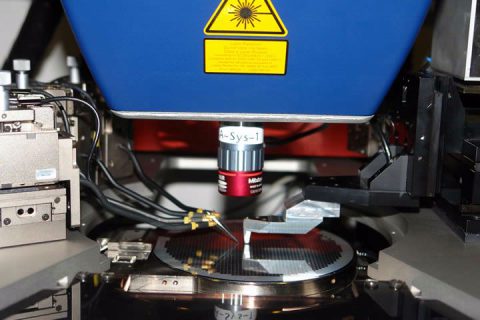
These platforms allow flexibility for wafer-level MEMs tests. They all can handle non-electric stimuli and detection instrumentation besides the standard electrical test interfaces.

October 26, 2017
These platforms allow flexibility for wafer-level MEMs tests. They all can handle non-electric stimuli and detection instrumentation besides the standard electrical test interfaces.
In an earlier blog post, we covered the first of several methods to test MEMS devices at wafer-level – pressure sensors – which includes pressure probe modules, a pressure chamber, and a dynamic test via stimulation with an electrostatic field. In this post, we’ll cover microphones, resonators, oscillators, RF switches, and microbolometers.
There are two different designs for microphones – top side contact with a top membrane and top side contact with a bottom side membrane excitation. Therefore, there are two different probe system setups that are required. There is a standard platform which provides top side noise stimulation and probe card contact with an integrated reference microphone. To stimulate the MEMs microphone from the bottom side, a double-sided probe system is used.
A specific uniform sound level is applied to stimulate the membrane. To integrate the reference microphone, a probe card is used for contacting. It can be used either on manual or automated probe systems. Furthermore, the typical parameters are sensitivity, which is measured in millivolt / Pascal (mV/Pa) and the frequency response in Hz.
With resonators, oscillators and RF MEMs, these types of devices are tested in a vacuum before packaging. Because these are operating in a vacuum environment, this testing is typically done in R&D (as example to evaluate damping properties) so pressure regulation is required. It is also possible to test with different gas concentrations. Probe cards with integrated read-out electronics or vacuum proof standard DC or RF probes can be used to contact the devices. To test under different temperatures, thermal chucks ranging from -60° C to 300° C can be used.
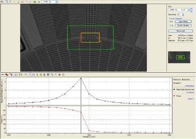
 The image shows the test results of a MEMs gyroscope. It is electrically stimulated and the resulting movement is optically detected.
The switching behavior of an RF MEMS can be tested under different conditions (as example vacuum, atmosphere or different gas concentrations). The RF equipment is based on the standard |Z| Probe® accessories and works down to cryogenic temperatures.
Uncooled infrared sensors, also called µBolometer are tested in a vacuum environment. Since they are working at room temperature, no thermal chuck is required. In general, it is possible to use a thermal chuck option between from -60° C to 300° C for R&D testing. Typically, the devices are diced and arranged on a 200 mm x 200 mm carrier plate. The single devices are individually aligned using our Velox™ probe station control software. It is also possible to test a full 200 mm wafer. For radiometric measurements, the device is illuminated by a black body, which is an ideal infrared source. Above the device, there is an adjustable aperture, or a filter can be used.
The above platforms, along with pressure sensors from our previous blog, allow flexibility for wafer-level MEMs tests. They all can handle non-electric stimuli and detection instrumentation besides the standard electrical test interfaces.