Wafer probers provide an established platform for performing electrical measurements at wafer level for CMOS and similar process technologies. For testing IR sensors, the requirements are beyond the standard prober capabilities. Wafer probers are used for taking electrical measurements at wafer level since the beginning of the semiconductor industry. The devices are contacted with probe needles to electrically measure their functionality. The prototype phase requires setup of test procedures, which lead into reduced testing in full production environment to detect device failures early in the fabrication process.
A platform for testing IR sensors at wafer level is based on standard probe stations but requires additional modules and functionality. The PAC200 is the ideal cryogenic probe solution for automatic testing of wafers and substrates up to 200 mm in a cryogenic environment down to 77 K with liquid nitrogen or below 20 K with liquid helium opening up possibilities for testing infrared sensors at cryogenic temperatures.
The Test Process
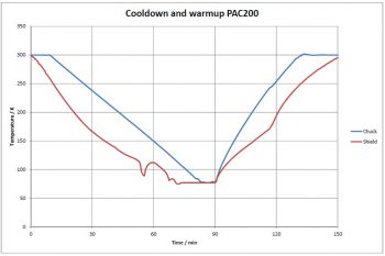 The test devices are placed on the carrier that is mounted to the cryogenic chuck. After loading this carrier into the test chamber, the ‘pump down’ process is started. When the target vacuum level of less than 1×10-³ mbar is reached, the ‘cool down’ process is started. It takes about 90 minutes to reach and stabilize at the test temperature of 77 K (see the chart below right – cool down and warm up process). The probe-to-pad alignment is set up once in the vision software and then executed after temperature stabilization. Depending on the device size, it has to be done once for aligning a wafer or several times for each individual die. Now the black body can be set to its target temperature and moved above the central view port. The measurement is executed after contacting the device with the prober needles. Depending on the test requirements, a second or third black body can be moved into the test position or the stage can step to the next device. This procedure is repeated until the last device has been tested. After that, the system is warmed up to room temperature and ambient pressure. The carrier can then be unloaded.
Here are four test examples:
1. The testing of flip-chip bonded hybrids. The most common test is the characterization of already bonded devices. The readout electronics could still be in wafer format of 150 mm or 200 mm size, or single chips. The chip requires a test environment similar to the work environment of the final product. For flip-chip bonded hybrids, this requires the electronics to be in close proximity to the sensor. This is done by embedding these electronic components into the probe card. A cryogenic probe card is based on standard technologies with further improvements to work at 77 K. The probe card is integrated into a compact probe card shutter unit. This unit is designed for production use to easily change between projects, which requires different probe cards, apertures or filters. The shutter allows changing between the different requirements during the testing cycle. For aligning the device under the needles, a free camera view through an open shutter position is needed. A filter glass only allows specific wave lengths passing the device while illuminating it with a black body for uniformity testing. The closed position is used for measurements in a completely dark environment.
2. The testing of single diodes. Besides the testing of the functional camera chip, single pixel diodes of the IR detector can be characterized. This can be done on the entire wafer or singularized substrates. The contact pads of these diodes are typically very small, down to a range below 10 µm. To achieve stable contact, special sharpened probe needles need to be used for testing. Single probe positioners provide a very flexible setup and are recommended for R&D work when pad arrangements frequently change. For production-like testing, for example, complete array measurements over several hours utilize a probe card-type needle setup. The copper-style needle housing is embedded into the cryogenic shield to guarantee minimum heat entrance to the device under test. An additional cover surrounding the probe card is coated black internally to avoid stray radiation influencing the measurement results. A shutter system is able to remotely switch between positions for camera view and a closed position for dark current measurements. Additionally, a filter glass can be integrated into a third position. These diode IV measurements require a very high current resolution down to the fA range. This is realized by a seamless triaxial test setup from the needle to the parameter analyzer. State-of-the-art measurement units provide the ability to control the probe station, do the measurements, and archive the results.
3. The testing of read out electronics (ROIC). This test is done by testing the entire wafer up to 200 mm in diameter before the detector array is bonded. It’s a basic electronic test to uncover functionality issues before the expensive detector material is bonded. For contacting the test pads, the same probe card can be used for hybrid testing.
4. A µBolometer test. The test of µBolometer requires only a vacuum environment. The test temperature is ambient. However, it can be useful to have a thermal chuck if an absolutely stable temperature is needed. A black-coated aperture and baffle design are integrated above the probe card. The probe card itself is made of high vacuum proof materials to avoid outgassing. A customized proximity electronic can be placed inside the chamber or right outside on the chamber top cover. The window glass is set to ZnSe due to the required wavelengths. To increase the transmission of the window, the glass can be customized with an anti-reflective (AR) coating.
Wafer probe systems are able to provide the required environment for IR sensor testing prior to packaging. The needed adaptations for the target test temperature, the device stimulation, and measurement accuracy are implemented and established as field-proven solutions.