Achieving accurate and continuous measurement for sub-THz wafer-level device characterization is particularly important for device modelling applications. Here, we share five challenges in making wafer-level measurements up to 750 GHz, and how to overcome them.
 Complex and Tedious Waveguide Sub-THz Test Setup
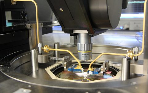
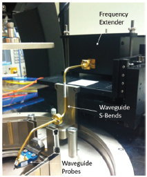
Preparing test systems to measure S-parameters of the same device from low frequencies to 750 GHz is a very tedious task as most network analyzers can only support up to 67 GHz. To extend measurement coverage to 750 GHz requires banded frequency extenders and banded waveguide probes shown in the figure to the right. Using these 6 sets of frequency extenders and probes to characterize the same device, the combined overall measured results is extremely prone to discontinuities. Modelling engineers face a perplexing task if they have to re-setup and re-measure the device at a particular frequency band. The frequency extenders and waveguide probes have to be re-mounted onto the probe positioners and the probe tips have to be re-calibrated before any measurements could be made. A post calibration validation method is urgently needed to minimize measurement discontinuities, the first time the device is tested at every individual frequency bands so as to avoid tedious re-measurements.
Post-Calibration Verification for Frequencies < 67 GHz
Inexperienced device modelling or test engineers are still making the mistake of validating their calibrated system with electrical standards that were used to calibrate the VNA. For applications up to 67 GHz, a 2-step verification is recommended. First, after calibration, the probes are lifted in the air and the OPEN return losses at Port 1 and Port 2 are measured. They are recommended to be within ±0.1dB. Being the most repeatable test, probes in the air can also be used to conveniently monitor the system drift over time. Next, verification lines such as 1ps transmission line is used to validate the accuracy of the measurement reference plane and monitor the contact resistance of the probe tips. Such verification must be performed after calibration as well as after completing all the device measurements to ensure accuracy and traceability of all measured data collected throughout the day.
Post-Calibration Verification at Sub-THz Frequencies
At sub-THz frequencies, post calibration verification is even more critical to ensure minimal measurement discontinuity and highest accuracy. Regardless of calibration methods adopted for the sub-THz wafer-level measurements, it is recommended to design verification lines on the calibration substrates (if probe tip calibration is used) or on wafers (if multi-line TRL is used). The figure 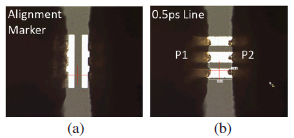 to the right shows an example of a verification line with probe alignment markers to help detect measurement discontinuity. The probe alignment marker (a) and 0.5ps verification line (b) on alumina substrate with waveguide probes.
Regardless of calibration method used, modelling engineers must characterize all their frequency extenders and test setup with a short verification line (on the calibration substrate or wafer) for optimal post-calibration validation at each frequency bands prior to characterization of devices to minimize measurement discontinuity. It is also recommended to fabricate multiple duplicates of such verification lines so that if they are worn out, new ones are readily available.
Probe Contact Resistance & DC Biasing Voltage
 There is a challenge in monitoring low frequency probe contact resistance since it is not possible to measure RS from second to the sixth frequency bands. This work proposes, prior to calibration, that device engineers measure the DC contact resistance of the waveguide probes for each frequency band to ensure probe contact resistances are consistently low and identical for all frequency bands. Signal and ground tips of the waveguide probes are placed on a common gold pad and the probe contact is measured with Kelvin sense probes. This is particularly important when measuring low resistive passive devices as waveguide probe tip can wear out with use, exhibiting abnormally high contact resistance which will result in measurement discontinuity.
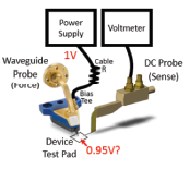
DC biasing voltage, when testing active devices such as transistors, are added through the built-in bias-tee in waveguide probes. These bias-tees have been optimized to perform specifically for each frequency bands. As such, to ensure identical DC voltage applied at the device test terminals, it is vital to adopt the setup in the figure to the left to measure the voltages at device test pads so that voltages drop across parasitic resistances of the DC cables, bias-tee and probe contacts are duly compensated. This will help ensure identical bias voltages on the device terminals for every frequency band to eliminate measurement discontinuities.
RF Source Power and Probe Tip Power Calibration
Probe tip power calibration is mandatory for active devices because source power set by device engineers on the VNA has no effects on the sub-THz frequency extenders, leading to incorrect and inconsistent source power applied to the device for different frequency bands [5]-[6]. Since S-parameters are relative measurements, most instrumentation and test engineers believe that probe tip power calibration is not required for passive devices. The paper linked below demonstrates for the first time that even for passive devices, having power at the probe tips calibrated for S-parameters measurements can actually reduce system drift over time, which is one of the key culprits in causing measurement discontinuities. A new probe tip S-parameter and power calibration approach is proposed. A single sweep 10 MHz-110 GHz system with a 67 GHz VNA is used in this work as it allows unbiased studies of power calibration and measurement discontinuities in a single setup, avoiding the need to change frequency extenders, RF probes and combining test data from two frequency bands.
To achieve accuracy and continuity in wafer-level sub-THz measurements from low frequency to 750 GHz, it is critical to ensure low probe contact resistance and accurate DC bias applied to the device for all frequency bands. The proposed post-calibration verification techniques in the paper, as well as performing probe tip power calibration with S-parameter calibration, are critical and have been shown in this work to eliminate sub-THz measurement discontinuities.