Constant Current Electromigration (CIEM) is coming under fire as a new interconnect reliability test methodology – Constant Voltage Electromigration (CVEM) – begins to take root. Many (including FormFactor) are seeing the shortfalls of CIEM alone for evaluating EM on highly scaled copper lines and vias. Some of the emerging challenges to CIEM revealed by interconnect technology evolution include:
- Rising statistical uncertainty, as process variability increases
- Undue pessimism, in a world with rapidly shrinking EM reliability margins
- Inappropriate void formation acceleration with multiple false failure events and unrealistic recovery mechanisms, in scaled interconnects where barrier conductivity is dropping significantly
Corrupted data and unnecessarily pessimistic conclusions lead researchers to look in other directions, and constant voltage EM deftly addresses each of these issues as a complementary, or perhaps replacement, test method. Here are the first two of five reasons that CVEM is a better reliability test methodology for today and tomorrow’s advanced interconnects:
- Tighter TTFs for Improved Extrapolation. The ITRS roadmap lists the roughness of lines and barriers among the top five most critical challenges for interconnects beyond 16 nm. Traditional CIEM will be challenged by this. CIEM applies a current bias to a sample set, stressing each device under test (DUT) with current density j = I / A, where I is the stress current and A is the sample’s cross-sectional area. Line edge roughness (LER) contributes to sample-to-sample differences in A and therefore creates inconsistency in the j values presented to the samples. These j errors unpredictably shift each individual DUT’s failure time, causing extra scatter in the lognormal plot as shown by an increased sigma (σ) shape parameter.
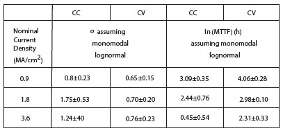 CVEM offers a solution to this unintentional error source, by specifying stress as an e-field E = ρ * j = V / l, where ρ is the resistivity of the structure material, V is the stress voltage, and l is the length of the structure. Errors in DUT length l are proportionally insignificant, and thus the stress bias is applied consistently across all samples and σ is unaffected by dimensional variability.
The table to the right presents a dramatic example where CIEM produced very high σ values compared to CVEM. The data are from a dual damascene copper structure with nominal line width of 40 nm from an as yet immature process with high cross-sectional area variation across the wafer; this test vehicle was chosen to exemplify the difference between test methods. High σ values not only reveal scattering in the failure times, but also impact lifetime predictions especially when extrapolating to lower failure rates.
As scaling reduction continues, dimensional process variability will proportionally deteriorate and increase the negative impact on σ. CIEM is appropriate for some qualification studies which need to see this variation; for many other studies, however, this could corrupt analysis enough to lead to erroneous conclusions. Fortunately, CVEM offers a natural insulation from increasing dimensional variation and stress bias corruption for a purer σ.
- More Accurate Failure Times. Accurate lifetime extrapolation is increasingly important, given the well-documented trend that EM lifetimes are dropping precipitously with each scaling node. There is little margin for unnecessarily gloomy predictions.
We’ll explore three more reasons CVEM is a logical replacement for CIEM for more accurate and reliable IC failure capture in our next post, so come back next week.