There are numerous shortfalls and challenges when using Constant Current Electromigration (CIEM) for IC failure capture, leading many in the industry to move toward Constant Voltage Electromigration (CVEM) as a more accurate and reliable test methodology to either complement or replace CIEM.
In our previous post we identified the first two of five reasons why CVEM is a better reliability test methodology for today and tomorrow’s advanced interconnects. To recap, they were:
 Tighter TTFs for improved extrapolation
- More accurate failure times
In this post, we’ll dive into the next three reasons to consider CVEM:
3. Correct Current Density Acceleration.
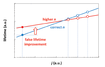
A possible hidden danger in CIEM is that it could have a worse overstress effect at higher current densities than at lower current densities (power is a function of the square of the current density). The consequence is that tests at higher j values are more incorrect, with fail times more strongly reduced, than those at lower j values. This leads to a higher calculated current density exponent, n, in Black’s Equation: MTTF = A0 * j-n * e(Ea/kT). Paradoxically, shorter fail times for CIEM stress data can actually lead to falsely optimistic lifetime predictions as diagrammed in the graph to the right.
Note that this higher n effect has not been conclusively identified; it was observed in some early studies, but not apparent in others. The 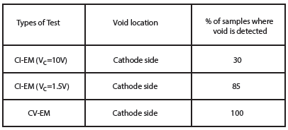 dependency of n on the failure mechanism and structure design complicates the confirmation of this concept, and further investigation is required.
4. More Investigative Tools for Failure Analysis.
One side effect of the CIEM overstress problem is that it is observed to obliterate the voids, denying researchers a valuable tool. In contrast, as seen here to the right, this useful evidence is much better preserved for failure analysis under CVEM.
5. Overcoming False Failure Phenomena.
Scaling progress demands ultra-thin barriers. These are needed to combat increasing surface scattering and loss of cross-sectional conductor area as trenches narrow. The proposed geometries and materials to maximize fractional conductor area and reduce copper resistivity point to increasingly resistive/non-conductive barriers.
This changes the nature of DUT behavior when void growth approaches an open-circuit condition, and especially highlights the problem of CIEM overstress described above. DUTs without a conductive barrier shunt path see a supercharged version of the overstress problem previously described. When the CIEM test method is used with a high voltage compliance (common for many EM test systems), the degrading DUT’s increasing resistance leads to very strong overstress conditions and heat in the vicinity of the void. It is conjectured that metal adjacent to the void becomes a reservoir source of material which may then fill or partially fill that void for a self-healing effect.
CVEM eradicates the multiple false failure phenomena to easily discern the true failure times.
We have created the industry’s first full-featured, high-performance, integrated CVEM test solution by providing a Multipurpose EM (MPEM) Module for our proven 1164 and Symphony™ reliability test systems. The MPEM Module delivers a number of very useful high-performance features such as full parallel high-speed DUT sampling, programmable voltage compliance, and a full suite of software functions.