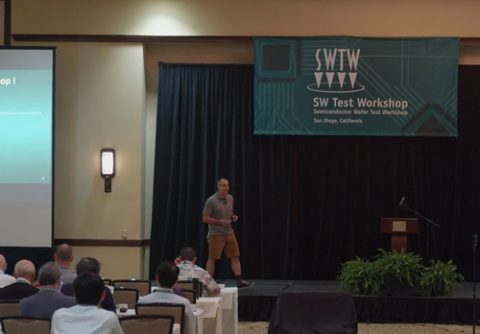
Join us at the Semiconductor Wafer Test Workshop (SWTW) on June 3rd – 6th in San Diego, California where we’ll be presenting three great presentations.
1. 5G: The Next Disruptive Technology in Production Test (Monday, June 4th – 9:30-10am)
The development of 5G / WiGig products are creating a unique challenge for high volume production testing of radio devices. These devices operate at multiple frequencies throughout the 24 GHz to 86 GHz range – well beyond the 6GHz RF capabilities of most existing production ATE ‘s. In addition, these devices may incorporate phase array beam-forming antennae which create additional challenges in a production test environment with high channel counts in excess of 24 per device. Design of the test solution requires creation of up/down converter circuits to reach 5G frequencies. These are required since the RF resources on the production testers have a 6 GHz limit. The millimeter wave RX / TX signals are generated by commercially available components mounted to the SIU/TIU and programmed with digital pins. Also, beam-forming requires that a single DUT have greater than 24 RF channels – well beyond what a tester and probe card could easily handle. Once this moves to HVM, the total number of a multi-DUT test cell will require more than 256 RF channels in a x8 parallel test.
WiGig devices have so far used radiated testing only. The resulting test solution has proven very reliable and robust and is currently running in high volume production. The test solution for testing of future 5G devices, as well as future WiGig products, will require testing of BGA, WL-CSP and DIE using both conducted and radiated methods in a full test cell. The final HVM test solution design needs to have low installation cost and high-volume test capabilities. Results will be presented that illustrate the initial testing of both conducted and radiated methods. In particular, the RF measurements are using our Pyramid Probe technology with both contacts and probe card antenna multiplexing in order to reduce the number of required RF channels.
2. Enabling High Parallelism in Production RF Test (Monday, June 4th – 4:30-5pm)
The proliferation of higher complexity RF devices and volume production of those devices presents a new combination of obstacles at wafer test. For example, Wi-Fi combo devices are typically larger die, incorporating multiple radios that require low loss electrical connections and robust mechanical contacts to measure their functional performance on wafer. Traditionally, device manufacturers have deployed probe cards that support high frequency signals or mechanically robust multi-site probe cards, but not both. Today’s widespread consumer demand for connectivity needs these two capabilities combined to achieve a reasonable cost of test. Probe cards now must support devices with high frequency signals en masse, must increase test efficiency through parallelism, and must hold up over time in a production environment.
Much of the technology to address today’s combined challenges has existed for years, but not in an integrated form. Certain pieces were missing altogether, including a frequency-capable vertical contact. Legacy Cascade Microtech Pyramid technology enables the use of transmission lines through almost the entirety of a probe head for excellent RF performance. Legacy FormFactor Katana MEMS technology enables robust, high parallelism contacts that are fully repairable, and provide millions of touchdowns. Combining these attributes with a new vertical probe head architecture results in a new tool – a truly production-worthy multi-site probe card initially supporting RF signals up to 10 GHz.
Together, we offer uptime and scalability that was previously limited to low frequency applications, and RF signal capability formerly limited to lower parallelism and limited use in production. To demonstrate the complementary effects of a Pyramid-style membrane space transformer and an RF-enhanced Katana head, we present results from a production evaluation of our Pyrana probe card.
3. Break the Myth of Wafer Probing on Cu for Fan-out Wafer Level Packaging (Tuesday, June 5th – 8-8:30am)
Fan-out Wafer Level packaging (FOWLP) is one of the fastest growing advanced packaging segments today. Its growth was ignited when Apple 7 A10 processor incorporated the fan-out techniques for the high-end mobile application processors. According to Yole Research, FOWLP is expected to grow to $2.5B by 2021.
FOWLP has introduced a significant shift in wafer level test requirement.
- Due to the ability of the fan-out nature, the native pitch for wafer test can potentially be reduced significantly to well below today’s 100um’ish pitch in production, down to 30-40um pitch range, for wafer testing prior to die singulation and fan-out.
- Higher quality of electrical test is demanded at wafer level prior to singulation to ensure only know-good-die go through the fan-out back-end processes. This has required higher level power integrity (PI) and signal integrity (SI) wafer level at wafer level.
- FOWLP process has also introduced new test insertion possibilities, where probing on Cu material directly is desired. Probing on Cu has been widely perceived to be challenging due to concerns with Cres stability due to rapid oxidation of Cu in air, especially at elevated temperature.
Samsung and FormFactor have collaborated in developing a new vertical MEMS technology to break the myth of “probing on Cu”. We have evaluated a new type of MEMS probe tip material that’s optimized for Cu probing. In the paper, we will present our evaluation process and promising results from the Cu probing process for FOWLP, as well as capabilities to support known-good-die testing and pitch reduction to sub-40um.
We will also be exhibiting and will be set up at Tent Booth #4 on Monday and Tuesday. Swing by and say hello! We hope to see you there!
