April 25, 2019
While on-wafer testing methodologies for GaN and SiC power semiconductors (lateral and vertical structures) are similar for Si devices, expanded test capabilities are needed for these newer wide band gap devices.
April 25, 2019
While on-wafer testing methodologies for GaN and SiC power semiconductors (lateral and vertical structures) are similar for Si devices, expanded test capabilities are needed for these newer wide band gap devices.
The demand for high-power devices (built on Si, GaN and SiC substrates) has been primarily driven by automotive and industrial segments such as hybrid and electric vehicles, solar, transportation, data center power supplies, and other industrial segments. While on-wafer testing methodologies for GaN and SiC power semiconductors (lateral and vertical structures) are similar for Si devices, expanded test capabilities are needed for these newer wide band gap devices.
When testing Si and advanced GaN/ SiC devices on-wafer instead of in-package, R&D engineers and test operators are faced with some major challenges to collect high accuracy data.
1. Anti-arcing for high voltages
Typically, when measuring high voltages on-wafer there will be electrical discharge (arcing) between probe needles. This also occurs between the DUT (device under test) and adjacent devices (vertical layouts) or other test pads (lateral layouts). In addition, arcing can occur between the wafer chuck and the surrounding probe station at voltages above 1000 V.
2. Low contact resistance of the probe to device
Another key challenge to achieving accurate high current measurements is to keep the contact resistance of the probe to device as low as possible. This will ensure that the full performance of the device can be measured on-wafer with full correlation to in-package performance. This leads to significantly lower costs using known good die for final end-application power modules.
3. Low contact and thermal resistance, with uniformity between wafer and chuck
To get accurate data for every device on the wafer, it is important to have uniform physical contact between the wafer backside and the chuck top surface. Firstly, this reduces thermal errors by ensuring full device-generated heat is distributed away from each device, no-matter the device location on the wafer. And secondly, for vertical devices (such as IGBT’s) where the chuck functions as one of the electrical contacts, this enables ultra-low contact resistance – a critical need in overcoming resistance errors for non-kelvin testing of RDS(on). Only when both challenges are solved can each device’s maximum performance be seen in testing data.
4. Accurate device models for Circuit Designers
A challenge for device characterization engineers is to measure both high voltage/high current AND accurate low leakage performance to create a complete device model. This will help circuit designers to optimize their power IC designs for maximum commercial value. Balancing high voltage/current switching versus device power consumption when not operating (off-state leakage) is a key focus of this work.
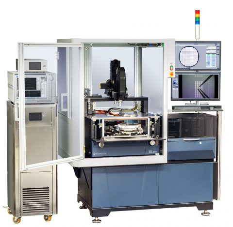
To meet these challenges, we created the TESLA200 Advanced On-Wafer Power Semiconductor Probing System for power semiconductor researchers, device/test engineers and manufacturing managers/operators. To learn more about TESLA200 probe system, visit our website, or download the data sheet(PDF).