In the world of advanced packaging, wafer test has become more important than ever. We are leading
the way with solutions for the toughest problems—today.
With the reality that Moore’s Law is approaching its practical end, our industry has applied its creativity towards advanced packaging to continue to achieve performance and cost goals. In the “Age of Data”, advanced packaging technologies offer breakthrough enhancements in computing power and memory bandwidth to support important initiatives such as artificial intelligence, automotive, 5G/mobile, high performance computing and other high-end applications. Companies like Intel, TSMC and Samsung are leading the way in blazing a path in new advanced packaging techniques.
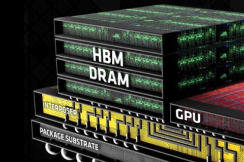
We define Advanced Packaging as 2.5D/3D heterogenous integrated packages where different types of die or chiplets are “glued” together through interposers or hybrid bonding processes to allow the various stacked die to communicate to each other and externally. These chiplets can be mixed and matched as needed to provide better overall performance and faster time-to-market.
Analogous to the Moore’s law transistor shrink, the “new” shrink for advanced packaging is the 2.5D/3D interconnect pitch reduction, to allow more information in and out of the die without increasing the die size. This, in turn, significantly reduces probe card pitch to test these devices. As we have seen in the last few years, the packaging bump pitch has reduced from 150um to today’s sub-50um.
FormFactor is at the forefront, with test and measurement solutions to reduce the manufacturing cost of advanced packages.
We help customers deliver high-confidence parts while balancing test complexity, coverage and cost. Our probe system (CM300) and advanced MEMS probe cards (SmartMatrix, Apollo, HFTAP, Altius) are used to verify electrical performance and yield, not only for the individual chips in the stack such as HBMs and processors, but also the fine-pitch interposers, as well as the package substrate and final stack to ensure the complete package works. Our products empower customers to gain more intelligence at any stage of the heterogenous integration process, where the traditional way to yield optimization on a monolithic silicon die is no longer adequate. If you can’t measure it, you can’t improve it.
Want to learn more? Read our CEO Mike Slessor’s article on Advanced Packaging in Semiconductor Digest or download his recent presentation at Semicon West’s TestVision. You can also download a technical presentation presented by Alan Liao at FormFactor’s Taiwan user group conference on the challenges of verifying HBM2 stacks.
Additionally, read the TSMC, Intel, and Samsung Advanced Packaging Overview which featured some visionary speakers (and customers) – Babak Sabi from Intel, Steve Hah from Samsung, and Marvin Liao from TSMC.