May 11, 2023
With the emergence of innovative technologies, such as integrating multiple dies into monolithic systems, meeting the increasing demand for cost-effective performance in top-end applications has become more challenging.
May 11, 2023
With the emergence of innovative technologies, such as integrating multiple dies into monolithic systems, meeting the increasing demand for cost-effective performance in top-end applications has become more challenging.
With the emergence of innovative semiconductor technologies, such as integrating multiple dies into monolithic systems, meeting the increasing demand for cost-effective performance in top-end applications has become more challenging. Moore’s Law alone can no longer guarantee price/performance advances, and new solutions are needed.
One such solution is advanced packaging technologies, which enable scaling and performance gains independent of on-chip feature size. Examples include High Bandwidth Memory (HBM), Fan Out Wafer Level Packaging (FOWLP), and Heterogeneous Integration (HI) technology like Intel’s system-in-package (SiP). These technologies require highly optimized and accurate fabrication processes to be cost-effective and achieve high-quality results. Each of the die and integration substrates used as components of a heterogenous stack must be ‘known’ to be fully functional, or if not, the manufacturer risks losing all of the dies in the stacked package, as well as the time and cost of assembly.
As a result, wafer-level test has become critical in multiple phases of the production process, and FormFactor is a key participant in developing advanced packaging technology. Our test and measurement solutions play an essential role in ensuring quality and help keep manufacturing costs under control.
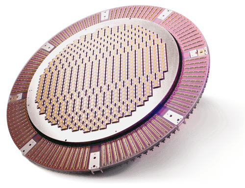
High Bandwidth Memory (HBM) is a cutting-edge technology that has revolutionized the memory industry, and it provides an excellent example of how wafer-level testing plays a critical role in the overall production flow. In recent years, HBM has become increasingly popular, particularly in high-performance computing and graphics applications, due to its outstanding bandwidth and power efficiency.
One of the most important features of HBM is the use of Through Silicon Vias (TSVs) linked by microbumps, which form the vertical pathways through the stack. TSVs are microscopic holes drilled through the silicon wafers, enabling communication between the DRAM layers and the logic layer. This technology has significantly increased the density of memory modules while reducing their power consumption and latency.
The underlying interposer layer connects the stacked components into a cohesive system, enabling high-speed communication between the various elements. The interposer also serves as a substrate for the TSVs, providing the necessary structural support for the stacked DRAM cores.
As the demand for higher bandwidth and greater power efficiency continues to grow, the role of wafer-level testing in the production of HBM and other advanced memory technologies will become increasingly critical. The integration of complex memory architectures, such as HBM, requires a high degree of precision and reliability in the wafer-level testing process to ensure the highest possible yields and quality. With continued advancements in testing technology and methodologies, wafer-level testing will undoubtedly play an even more significant role in the production flow of next-generation memory technologies. Similarly, as other diverse device types are integrated together with memory into a single package, wafer-testing of each component is imperative to ensure the quality and function of the combined multi-part chip.
Although the influence of Moore’s Law on the IC industry may be waning, there is still an unrelenting need for more powerful micro-circuitry. As 5G technology becomes more prevalent, data centers must prepare for a deluge of information flow. The utilization of AI for deep learning is set to consume CPU cycles at an unprecedented rate. Additionally, virtual reality is poised to push graphics to new heights, while autonomous vehicles require exceptional real-time performance and near-flawless reliability.
At FormFactor, we are prepared and committed to doing our part to ensure that the semiconductor industry keeps up with this rapidly evolving world.