March 7, 2024
The application of superconducting resonator measurements exemplifies the role of PCM in the development of quantum devices, showcasing principles that could be applied across various domains to elevate device quality and yield.
March 7, 2024
The application of superconducting resonator measurements exemplifies the role of PCM in the development of quantum devices, showcasing principles that could be applied across various domains to elevate device quality and yield.
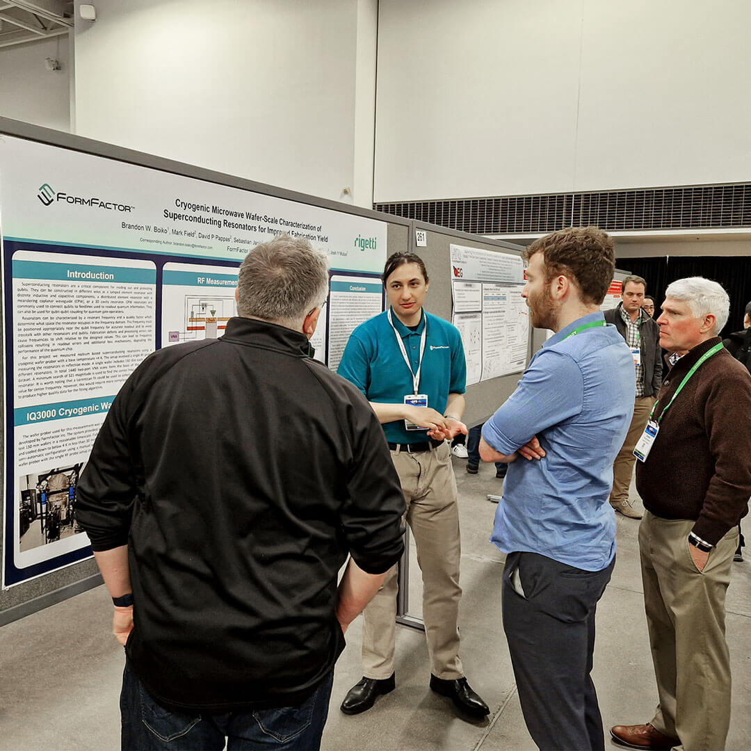
FormFactor’s Brandon Boiko presented Cryogenic Microwave Wafer-Scale Characterization of Superconducting Resonators for Improved Fabrication Yield at the APS March Meeting this week. Here’s an overview of that presentation.
Superconducting resonators play an essential role in the readout and protection of qubits, featuring various designs such as lumped element resonators with separate inductive and capacitive components, distributed element resonators with meandering coplanar waveguides (CPW), or 3D cavity resonators. CPW resonators, in particular, are frequently employed to connect qubits with feedlines for quantum information readout and facilitate qubit-qubit interactions necessary for quantum gate operations.
The performance characteristics of resonators, including their resonant frequency and quality factor, are critical as they define the resonator’s operational bandwidth in the frequency domain. The resonant frequency needs to be carefully aligned with the qubit frequency to ensure precise readout while minimizing interference with other resonators and qubits. Manufacturing inconsistencies and errors can lead to unintended shifts in frequency, potentially causing overlaps that result in readout inaccuracies and additional loss mechanisms, thereby affecting the quantum chip’s efficacy.
In this project, we analyzed niobium-based superconducting resonators at cryogenic temperatures below 4 K, using a cryogenic wafer prober. The experimental setup consisted of a single RF probe conducting reflection mode measurements across 160 dies on a wafer, each containing 9 different resonators, totaling 1440 two-port VNA scans for the statistical analysis. To identify each resonator’s center frequency, we employed a minimum search of the S21 magnitude. It’s noteworthy that applying a Lorentzian fit could yield more precise center frequency values but would necessitate a more complex calibration process to generate higher fidelity data suitable for the fitting algorithm.
For these measurements, the FormFactor HPD IQ3000 Cryogenic Wafer Prober, was utilized. This system enabled the automated testing of 150 mm wafers within a cryogenic setting on a practical timescale. Wafers were fully inserted into the device and reached temperatures below 4 K in under 30 minutes. On one side, the cryogenic wafer prober featured a semi-automatic setup, incorporating a manual wafer load arm. On the opposite side, the device’s cold chamber housed the single RF probe arrangement, all encased within a passive magnetic shield.
Today’s quantum computers, based on superconducting technology, are transitioning from laboratory-based development to industrial-scale production. Insights from the established semiconductor industry highlight the critical steps needed for success, including Process Control Monitoring (PCM). PCM is essential in any manufacturing process to meet design specifications and produce quality chips, with the added benefit of identifying defective devices early, leading to considerable cost savings. Additionally, implementing volume wafer testing as an intermediate process step can help adjust processes in real time and enhance overall yield.
We showcased a wafer-scale RF measurement technique for superconducting microwave resonators, gathering a comprehensive statistical dataset on resonator frequencies using a cutting-edge cryogenic wafer prober. Measurements were conducted using cryogenic RF probes and components to facilitate a two-port resonator assessment in reflection mode. By juxtaposing histograms of each resonator type, we could swiftly pinpoint frequency deviations and potential overlaps. A heatmap provided a visual representation of the dataset across an entire wafer, aiding in the detection of patterns that could signal which specific manufacturing steps require scrutiny.
Looking ahead, future endeavors could focus on refining these measurements through cryogenic calibration, enhancing data quality and enabling the use of Lorentzian fitting algorithms for more precise center frequency extraction and reduced measurement inaccuracies. Another area of exploration involves introducing an intermediary process step to adjust resonators post-measurement, aiming for tighter frequency distributions and significantly higher device yields.
The application of superconducting resonator measurements exemplifies the role of PCM in the development of quantum devices, showcasing principles that could be applied across various domains to elevate device quality and yield. Advancements in wafer probing technology promise to open up new possibilities, especially for applications that require low-temperature conditions.