December 3, 2025
Our long-standing collaboration set the stage for a major breakthrough: the world’s first silicon photonics prober for on-wafer measurements, a milestone that’s helping speed innovation across the SiPh landscape.
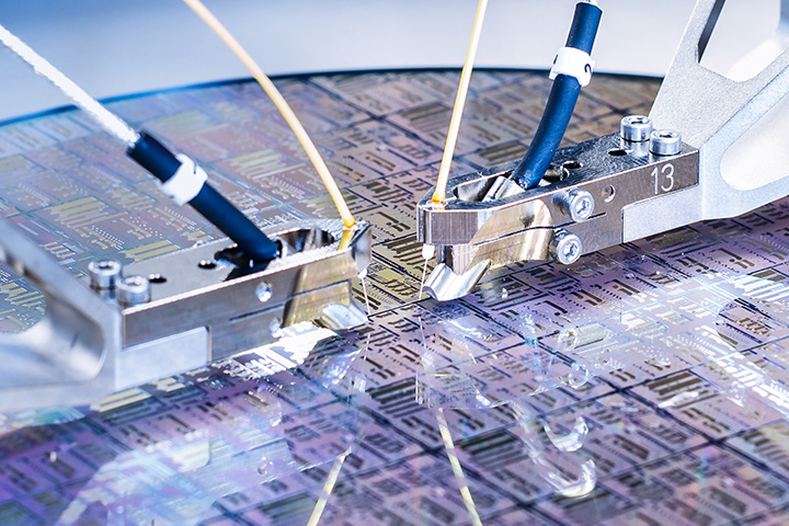
December 3, 2025
Our long-standing collaboration set the stage for a major breakthrough: the world’s first silicon photonics prober for on-wafer measurements, a milestone that’s helping speed innovation across the SiPh landscape.
As the demand for faster processing, lower energy use, and more complex photonic devices grows, Silicon Photonics (SiPh) has become a cornerstone technology. But for years, engineers lacked a dependable way to test these sophisticated chips at the wafer level. The precision required, often at micrometer scales, made traditional testing slow, inconsistent, and unable to keep up with real-world production needs.
FormFactor and the IHP Leibniz Institute for High Performance Microelectronics recognized this challenge early. Our long-standing collaboration set the stage for a major breakthrough: the world’s first silicon photonics prober for on-wafer measurements, a milestone that’s helping speed innovation across the SiPh landscape.
A Breakthrough Born from Collaboration
IHP contributed advanced test structures and real-world performance requirements, while FormFactor brought deep engineering expertise and automation capabilities. Working side-by-side, the teams transformed years of shared knowledge into a practical solution built for the complexity of next-generation photonic integrated circuits (PICs).
What once required slow, hands-on work is now an automated, precise, and repeatable process, delivering far greater accuracy in a fraction of the time.
Key Achievements at a Glance
The result of this partnership is a patented, industry-leading silicon photonics probing system that performs in hours what used to take days or even months. It gives researchers, designers, and manufacturers the ability to move faster, validate more accurately, and bring cutting-edge photonic technologies to market with confidence.
More than anything, this success story highlights what’s possible when long-term collaboration and practical engineering come together to solve real industry challenges.
You can review the comprehensive customer success story here.