There is a migration from Si to wide band gap substrate materials (GaN and SiC), that promises significant power semiconductor performance gains. According to Yole Developpement in their Power GaN report, in the next four to five years, the use of these materials is projected to grow by up to 3.9% ($1.7 billion).
In general, SiC and GaN high power semiconductors can operate at higher temperatures and with greater efficiency. Specifically, research and development for GaN is interesting for faster switching and SiC for high temperature applications. Devices that can support higher temperatures allow increased reliability, for automotive electric vehicles as example. Devices that can support faster switching enable lower energy loss. Both GaN and SiC based devices can be smaller than Si based devices which results in smaller packaging into consumer products.
When testing Si and advanced GaN/ SiC devices on-wafer instead of in-package, R&D engineers and test operators are faced with some major challenges to collect high accuracy data. These include the need for probe and system anti-arcing at high voltage, low resistance probe and wafer contacts for high current, and special handling for thinned wafers. Simultaneously, the need for “fast time to accurate data“ requires quick and easy setup of complex high-power test configurations. And, with operator and device safety in mind.
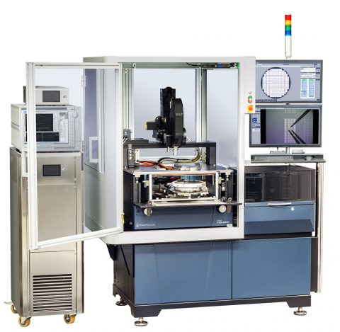
The TESLA200 Advanced On-Wafer Power Semiconductor Probe Station is an integrated high-power test solution that enables collection of accurate high voltage and high current measurement data, with complete operator safety.
Testing can be done on single or volume thinned wafers over a full thermal range of -55° up to 300° C and higher. The TESLA200 probe station allows easy setup and new test capabilities for static and dynamic high-power measurements in addition to ultra-low leakage device testing. Multiple anti-arcing technologies enable high-voltage test performance with superior device protection up to 10,000V DC.
In addition, very low contact/thermal resistance materials and technologies are integrated into the on-wafer probe system for best-in-class high-current measurements up to 600A. We complete the solution with an extensive range of high-voltage and high-current probes, and anti-arcing probe cards.
For more information, visit our website, or check out the latest TESLA200 Probe System video below.